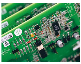
The needle bed is also called ICT test fixture, which is online inspection and test fixture. It is a non-standard test auxiliary fixture that uses electrical performance to test online components to check manufacturing defects and component defects. The PCB patch processing plant pointed out that it is mainly used to check the online single components and the open, short circuit, and welding conditions of each circuit network. It has the characteristics of simple operation, fast and rapid, and accurate fault location. The ICT test fixture can be simulated Device function and digital device logic function test, fault coverage rate is high, a special needle bed needs to be made for each kind of single board, this needle bed is called ICT test fixture in industrial production.
Needle bed (ICT test fixture) is divided into single-sided and double-sided, universal top plate is convenient for switching types, using adjustable bearing, easy to maintain, using acrylic & bakelite & FR-4 material (or designated), direct Gerber file processing generates drilling files to ensure drilling accuracy. The test program is automatically generated to avoid the possibility of manual input errors.

It is suitable for HP, Teluda, Zhenhua concord, SRC and other ICT models. The center distance between the two measured points or the measured point and the pre-drilled hole shall not be less than 0.050" (1.27mm). It is better to be greater than 0.100" (2.54mm), followed by 0.075" (1.905mm).
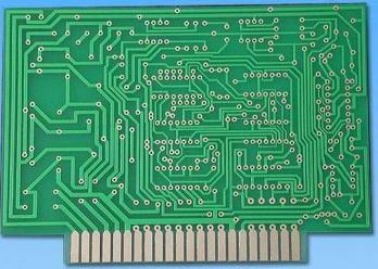
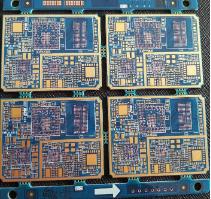
Needle bed test PCB circuit board:
However, with the evolution of technology, PCB size has become smaller and smaller. It is already a bit difficult to squeeze so many electronic parts on a small circuit board. Therefore, the problem of test points occupying circuit board space is often on the design side. There is a tug-of-war with the manufacturing side, but this topic will be discussed later when there is a chance. The appearance of the test point is usually round, because the probe is also round, which is easier to produce, and it is easier to get the adjacent probes closer, so that the needle density of the needle bed can be increased:
1.
The use of a needle bed for circuit testing has some inherent limitations on the mechanism. For example, the minimum diameter of the probe has a certain limit, and the needle with too small diameter is easy to break and damage.
2.
The distance between the needles is also limited, because each needle must come out of a hole, and the back end of each needle must be soldered with a flat cable. If the adjacent holes are too small, except for the gap between the needles There is the problem of contact short circuit, and the interference of the flat cable is also a big problem.
3.
Needles cannot be implanted next to some tall parts. If the probe is too close to the high part, there is a risk of collision with the high part and cause damage. In addition, because of the high part, it is usually necessary to make holes in the needle bed of the test fixture to avoid it, which indirectly makes it impossible to implant the needle. Test points for all parts that are increasingly difficult to accommodate on the circuit board.
4.
As the boards are getting smaller and smaller, the number of test points has been repeatedly discussed. Now there are some methods to reduce test points, such as Net test, Test Jet, Boundary Scan, JTAG. . Etc.; there are other test methods that want to replace the original needle bed test, such as AOI, X-Ray, but it seems that each test cannot replace ICT 100%.
Regarding the ability of ICT to implant needles, you should ask the matching PCB fixture manufacturer, that is, the minimum diameter of the test point and the minimum distance between adjacent test points. There is usually a desired minimum value and a minimum value that the ability can achieve. Large-scale manufacturers will require that the distance between the minimum test point and the minimum test point cannot exceed a few points, otherwise the jig will be easily damaged.