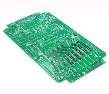
IC packaging substrate - PCB background technology
With the development trend of miniaturization, portability, multi-function, low power consumption and low cost of electronic products, 2D (two-dimensional) packaging technology has been unable to meet the requirements, and some products have begun to develop in the direction of 2.5D or 3D packaging. In 2.5D or 3D packaging structure, the combination of silicon-based adapter board and organic substrate is an important way to realize the interconnection between chip and chip, chip and substrate.
The traditional PCB manufacturing process of TSV adapter substrate is as follows: 1) making blind holes on the substrate; 2) The passivation layer on the side wall of the through hole was deposited by PECVD on one side of the substrate; 3) Through hole sidewall adhesion / diffusion barrier layer and seed layer metal were deposited on the substrate by single-sided magnetron sputtering; 4) Through hole metal filling is completed by electroplating process; 5) Through hole metal flattening; 6) The through-hole metal on the back of the substrate is exposed by thinning; 7) Make metal wiring, pad and its protective layer.
The traditional TSV transfer IC substrate preparation method has the following defects or shortcomings:
(1) The uniformity of passivation layer on the side wall of deep hole deposited by PECVD is poor. The thickness of insulating layer at the bottom of deep hole is only about 1 / 5 of that at the top, and the coverage of insulating layer at the bottom is poor. It is easy to produce discontinuous defects, which seriously affects the insulation effect and reliability. This also limits the depth width ratio deposition ability of passivation layer deposition process;
(2) The uniformity of adhesion / diffusion barrier layer and seed layer on the side wall of deep hole deposited by magnetron sputtering is poor. The thickness of the bottom of deep hole is only about 1 / 5 of that of the top. The coverage of the bottom of deep hole is poor. It is easy to produce discontinuous defects and lead to cavities during electroplating, which seriously affects the reliability of through hole. At present, the deposition capacity of the most advanced magnetron sputtering equipment is less than 15:1, which limits the deposition capacity of TSV;
(3) When the aspect ratio of deep hole is 20:1-30:1, it is difficult to realize the hole free electroplating filling process, and the large aperture will occupy the assembly area of components and reduce the wiring area, which is not conducive to high-density packaging;
(4) Limited to the traditional TSV transfer substrate manufacturing process, the thickness of transfer substrate is usually less than 200 μ m. It can only be used as a transfer substrate and cannot be directly assembled with the whole board;
(5) The cost of TSV adapter board is high, and the packaging process is complex, so it has no cost advantage in many packaging technologies;
(6) TSV adapter plate has the reliability problem because of the physical difference between silicon and organic substrate material, so it is difficult to integrate the structure;
(7) The ordinary organic substrate can meet the general density packaging requirements, but it can not achieve the packaging requirements of ultra-high density (such as lower than 55um interval bump reverse mounting).
The purpose of the utility model is realized as follows
The structure of a ic packaging substrate comprises a common substrate, wherein the upper surface of the common substrate is provided with a plurality of pads I, and the lower surface is provided with a plurality of pads II,
It also includes ultra-high density substrate, high-density chip, low-density chip and encapsulation layer I. the encapsulation layer I is arranged on the upper surface of the ordinary substrate. The ultra-high density substrate is composed of several layers of high-density rewiring metal layers and an insulating layer selectively spaced between them, and the upper surface is provided with a pad, Two or more layers of the high-density rewiring metal layers are selectively electrically connected with each other, the ultra-high density substrate is embedded in the encapsulation layer I, and its upper surface and pad are exposed from the encapsulation layer I, and part of the pad on the upper surface of the ultra-high density substrate is inversely connected with the high-density chip, Several outer metal electrodes of the substrate are formed outside the vertical area of the high-density chip, the upper surface of part of the outer metal electrode of the substrate is inversely connected with the low-density chip, and the lower surface of the outer metal electrode of the substrate is connected with the partial pad I of the common substrate through the blind hole penetrating the packaging layer I and the metal in the blind hole, A part of the lower surface of the outer metal electrode of the substrate is connected with a part of the pad of the ultra-high density substrate, and the pad II is provided with a solder bump. The line width / line distance of the high density rewiring metal layer of the ultra-high density substrate of the utility model is less than 6 / 6um. Alternatively, the line width / line distance of the high density rewiring metal layer of the ultra-high density substrate is 5 / 5um, 3 / 3um or 1.8 / 1.8um. The number of layers of the high-density rewiring metal layer of the ultra-high-density substrate of the utility model is more than five. Alternatively, the number of layers of the high-density rewiring metal layer of the ultra-high density substrate is 6, 7 and 8. The utility model also comprises an encapsulation layer II, which covers the exposed parts of the high-density chip, the low-density chip, the high-density substrate, the encapsulation layer I and the outer metal electrode of the substrate. Alternatively, it also includes a through hole, the through hole penetrates the cladding layer I and the common substrate, the inner part of the through hole is filled with metal, and the lower surface of part of the outer metal electrode of the substrate is connected with the partial pad II of the common substrate through the metal in the through hole.
The beneficial effect of the utility model is that:
The mixed density packaging substrate structure of the utility model adopts the ultra-high density organic substrate instead of Si interposer, and is embedded into the common organic substrate structure to provide smaller linewidth / line distance and more layers of high-density rewiring metal layer, so as to integrate and package multiple high-density chips and low-density chips within the same packaging area, It can not only effectively shorten the information transmission path, but also realize more functions, higher power and more leads, which is conducive to faster signal transmission, so as to adapt to the rapid improvement of semiconductor IC components in high speed, high frequency and large capacity, and further reduce the overall package thickness, It is a cost-effective and flexible packaging technology to adapt to many high-performance applications affected by space;
The utility model makes full use of the flexible characteristics of the ultra-high density substrate, improves the packaging reliability, and is conducive to the improvement of the product yield.
Among them: ultra high density substrate 10, outer metal electrode 110, blind hole 150, through hole 170, ordinary substrate 20, pad I 230, pad II 250, solder ball 251, cladding layer I 310, cladding layer II 430, high density chip 51, low density chip 53, cladding layer II 610.

Specific implementation mode example
Common ic substrate 20 generally refers to the basic materials for ic manufacturing electronic packaging substrate and motherboard carrying electronic components. It has three functions of conducting, insulation and supporting. Generally, the substrate is copper clad laminated plate. Through selective hole processing, chemical copper plating, copper plating, etching, etc., the circuit graphics are obtained on the substrate, and several pads i230 and several pads 2 250 are formed on the upper surface of common substrate 20. Generally, the width / line distance of metal layer of common substrate 20 is 40/40um, 20/20um and 8/8um, and the line width / line spacing can be achieved by 10/10um in the limit situation. The structure of the packaging substrate of the utility model is arranged above the common substrate 20 with a super high density substrate 10 having flexible characteristics. The ultrahigh density substrate 10 is composed of several layers of high-density re wiring metal layer and the insulation layer selectively spaced between them. There is selective electrical connection between two or more high-density re wiring metal layers. The welding pad is set on the upper surface of the ultra-high-density substrate 10, which has the characteristics of light, thin, falling resistance and high shape plasticity. It can be seen that compared with ordinary substrate 20, the width / line distance of UHD substrate 10 is smaller, the number of layers of high-density re wiring metal layer is more, and the unit area re wiring metal layer is more dense. Therefore, it is called ultra-high-density substrate 10, whose total thickness is no more than 100um, which is conducive to reducing the overall ic packaging thickness.
The packaging substrate of the utility model adopts the wafer level processing technology, does not need to use the complicated TSV process, avoids a series of problems such as deep hole electroplating process, and the application of the flexible ultra-high density ic substrate 10 improves the packaging reliability, which is conducive to the improvement of product yield.