Design method of printed circuit board in Shenzhen PCBA processing
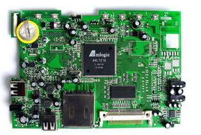
Printed circuit boards are also known as PCB circuit boards. Shenzhen PCBA processing is to process the PCB as the raw material and then process the electronic components required for welding on the PCB board through SMT or plug-in processing, such as IC, resistors, capacitors, crystal oscillators, and transformers. When the electronic components are heated at high temperature in the reflow oven, the mechanical connection between the components and the PCB board will be formed, thereby forming a PCBA.
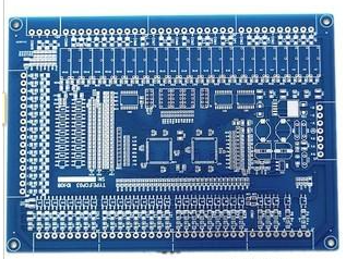
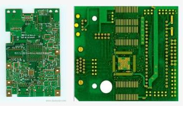
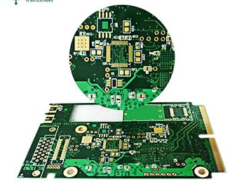
Printed circuit board is a necessary homework for electronic engineers to do electronic design. Shenzhen PCBA processing summarizes some design methods in the process of printed circuit board: One, the size of the printed circuit board and the layout of the device
The size of the printed circuit board should be moderate. If it is too large, the printed line will be long and the impedance will increase, which will not only reduce the noise resistance, but also increase the cost; if it is too small, the heat dissipation will not be good, and it will be easily interfered by adjacent lines. In terms of device layout, like other logic circuits, the devices related to each other should be placed as close as possible so that a better anti-noise effect can be obtained. Clock generators, crystal oscillators, and CPU clock input terminals are all prone to noise, so they should be closer to each other. It is very important that noise-prone devices, low-current circuits, and high-current circuits should be kept away from logic circuits as far as possible. If possible, separate circuit boards should be made.

2. Decoupling capacitor configuration
In the DC power supply circuit, the change of the load will cause the power supply noise. For example, in digital circuits, when the circuit changes from one state to another, a large spike current will be generated on the power line, forming a transient noise voltage. The configuration of decoupling capacitors can suppress noise caused by load changes, which is a common practice in the reliability design of printed circuit boards.
The configuration principles are as follows:
A 10-100uF electrolytic capacitor is connected across the power input terminal. If the position of the printed circuit board allows, the anti-interference effect of using an electrolytic capacitor above 100uF will be good.
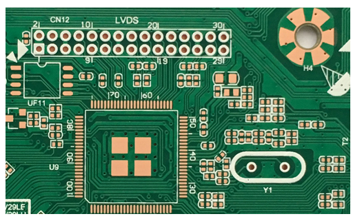
Configure a 0.01uF ceramic capacitor for each integrated circuit chip. If the printed circuit board space is small and cannot be installed, one 1-10uF tantalum electrolytic capacitor can be configured for every 4-10 chips. The high-frequency impedance of this device is particularly small, and the impedance is less than 1Ω in the range of 500kHz-20MHz. And the leakage current is very small (less than 0.5uA).
For devices with weak noise capability and large current changes during turn-off, and storage devices such as ROM, RAM, etc., a decoupling capacitor should be directly connected between the power line (Vcc) and ground (GND) of the chip.
The leads of decoupling capacitors cannot be too long, especially high-frequency bypass capacitors.
2. Ground wire design
In electronic equipment, grounding is an important method to control interference. If the grounding and shielding can be properly combined and used, most of the interference problems can be solved. The ground structure of electronic equipment roughly includes system ground, chassis ground (shield ground), digital ground (logical ground), and analog ground. The following points should be paid attention to in the ground wire design:
1, the correct choice of single-point grounding and multi-point grounding
In the low frequency circuit, the working frequency of the signal is less than 1MHz, its wiring and the inductance between the devices have little influence, and the circulating current formed by the grounding circuit has a greater influence on the interference, so one point grounding should be adopted. When the signal operating frequency is greater than 10MHz, the ground wire impedance becomes very large. At this time, the ground wire impedance should be reduced as much as possible, and the nearest multiple points should be used for grounding. When the operating frequency is 1~10MHz, if one-point grounding is used, the length of the ground wire should not exceed 1/20 of the wavelength, otherwise the multi-point grounding method should be used.
2, separate the digital circuit from the analog circuit
There are both high-speed logic circuits and linear circuits on the circuit board. They should be separated as much as possible, and the ground wires of the two should not be mixed, and they should be connected to the ground wires of the power supply terminal. Try to increase the grounding area of the linear circuit as much as possible.
3, try to thicken the ground wire
If the ground wire is very thin, the ground potential will change with the change of the current, causing the timing signal level of the electronic equipment to be unstable and the anti-noise performance to deteriorate. Therefore, the grounding wire should be as thick as possible so that it can pass the allowable current on the printed circuit board. If possible, the width of the ground wire should be greater than
4. When the ground wire is formed into a closed loop, when designing the ground wire system of a printed circuit board composed of only digital circuits, making the ground wire into a closed loop can significantly improve the anti-noise ability. The reason is that there are many integrated circuit components on the printed circuit board, especially when there are components that consume a lot of power, due to the limitation of the thickness of the ground wire, a large potential difference will be generated on the ground junction, resulting in a decrease in the anti-noise ability, If the grounding structure is formed into a loop, the potential difference will be reduced and the anti-noise ability of electronic equipment will be improved.
Our electronics focus on PCBA manufacturing, PCBA SMT chip processing, PCBA DIP plug-in processing, PCBA post-welding, DIP plug-in processing, Shenzhen DIP plug-in, PCBA, PCBA processing, PCBA OEM processing, Shenzhen PCBA plus electronic wire structure manual welding and shell assembly factory.