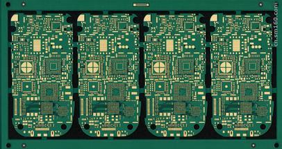
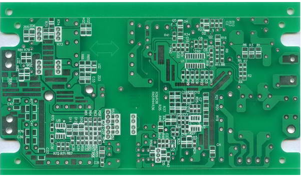
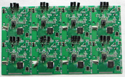
The main purpose of PCBA patch processing is to accurately mount the surface mount components on the fixed position of the PCB, and some process problems sometimes occur during the patch processing, which affect the quality of the patch, such as the displacement of the components. The displacement of the components in the patch processing is the foreshadowing of several other problems in the welding process of the component plates, which needs to be paid attention to. So what is the reason for the displacement of components in SMT processing? The reason for the displacement of the components in the patch processing: the use time of the solder paste is limited. After the use period is exceeded, the flux in it will deteriorate and the soldering will be poor. The viscosity of the solder paste itself is not enough, and the components are shifted due to the oscillation and shaking of the components during transportation. The flux content in the solder paste is too high, and the excessive flux flow during the reflow soldering process causes the components to shift.

PCB components are shifted due to vibration or incorrect handling during the handling process after printing and placement. During the patch processing, the air pressure of the suction nozzle was not adjusted properly, and the processing pressure of Shanghai smt was not enough, which caused the components to shift. The mechanical problem of the placement machine itself caused the wrong placement of the components. Once the component shift occurs in the chip processing, it will affect the performance of the circuit board. Therefore, it is necessary to understand the cause of the component shift during the processing and solve it in a targeted manner. The printing process is one of the key processes to ensure the quality of surface assembly. According to statistics, on the premise that the PCB design is correct and the components and PCB quality are guaranteed, 70% of the quality problems in surface assembly are caused by the printing process. Therefore, whether the circuit board processing and printing position is correct (printing accuracy), the amount of solder paste, whether the amount of solder paste is uniform, whether the solder paste pattern is clear, whether there is adhesion, whether the surface of the printed board is smeared by the solder paste, etc. Affect the welding quality of surface mount boards.
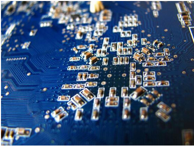
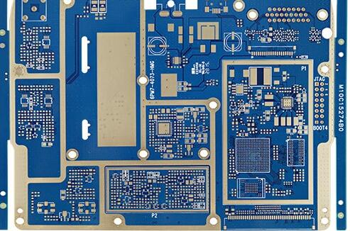
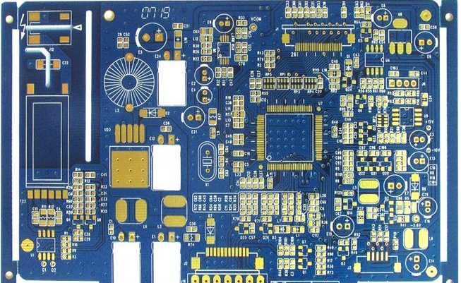
In order to ensure the quality of PCBA patch assembly, the quality of printed solder paste must be strictly controlled. (Narrow-pitch devices with a lead center distance of less than 0.65mm must be fully inspected). The amount of solder paste applied is uniform and consistent. The solder paste pattern should be clear, and try not to stick between adjacent patterns in the circuit board processing. The solder paste pattern should be consistent with the land pattern, and try not to be misaligned. The weight of the solder paste printed on the PCB is allowed to have a certain deviation compared with the weight value required by the design. The area of each pad covered by the solder paste should be more than 75%. After the solder paste is printed, there should be no serious collapse, neat edges, PCBA dislocation not more than 0.2mm, and for narrow-pitch component pads, electronic processing dislocation is not more than 0.1mm. The PCB must not be contaminated by solder paste. According to the company's standards or refer to other standards (such as IPC standards or SJ/T10670-1995 surface assembly process general technical requirements and other standards).