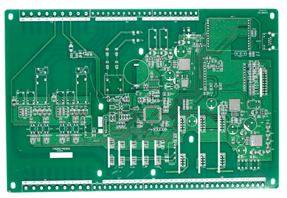
Diode PCB parallel termination
In some cases, Schottky diodes or fast switching silicon tubes can be used for transmission line termination, provided that the switching speed of the diode must be at least 4 times faster than the signal rise time. In the case that the impedance of the breadboard and the bottom board is not easy to determine, the use of diode termination is convenient and time-saving. If you find ringing problems during system debugging, you can easily add diodes to eliminate them.

Typical diode termination. The low forward voltage drop Vf (typically 0.3 to 0.45V) of the Schottky diode clamps the input signal between GROUND-Vf and VCC+Vf. This significantly reduces the overshoot (positive spike) and undershoot (negative spike) of the signal. In some applications, only one diode can be used.
The advantage of diode termination is that the diode replaces the Thevenin termination or RC termination that requires resistors and capacitors, and the overshoot and undershoot are reduced by diode clamping, without the need for line impedance matching. Although the price of the diode is higher than the resistance, the overall layout and routing overhead of the system may be reduced because it is no longer necessary to consider precise control of the impedance matching of the transmission line. The disadvantage of diode termination is that the switching speed of the diode is generally difficult to achieve fast, so it is not suitable for higher-speed systems.
(2) PCB serial termination
The PCB serial termination is achieved by inserting a resistor RS (typically 10Ω to 75Ω) into the transmission line in the PCB as close to the source as possible. The PCB serial termination is to match the impedance of the signal source. The resistance of the inserted PCB serial resistance plus the output impedance of the drive source should be greater than or equal to the transmission line impedance (slightly over-damped). That is to say, this strategy suppresses the signal reflected from the load by making the source end reflection coefficient zero (the load end is input with high impedance and does not absorb energy) and then reflected back from the source end to the load end.
The advantage of PCB serial termination is: each line only needs one termination resistor, no need to be connected to the power supply, and low power consumption. When driving a high capacitive load, it can provide a current limiting effect, which can help reduce ground bounce noise. The disadvantage of PCB serial termination is that when the signal logic is converted, due to the partial pressure of RS, a half-wave amplitude signal will appear at the source end. This half-wave amplitude signal propagates along the transmission line to the load end, and then from the load. The end is reflected back to the source end, and the duration is 2TD (TD is the transmission delay from the source end to the end of the signal), which means that no other signal input ends can be added along the transmission line.