In 1936, Austrian Paul Eisler (Paul Eisler) first used a printed circuit board in the radio. In 1943, Americans mostly used this technology for military radios. In 1948, the United States officially approved this invention for commercial use. Since the mid-1950s, printed circuit boards have only begun to be widely used.
Before the advent of the PCB, the interconnection between electronic components was done directly by wires. Nowadays, wires exist only for experimental applications in laboratories; printed circuit boards have definitely occupied the position of absolute control in the electronics industry.
In order to increase the area that can be wired, more single- and double-sided wiring boards are used in multilayer boards. Use one double-sided as the inner layer, two single-sided as the outer layer or two double-sided as the inner layer and two single-sided as the outer layer of the printed circuit board.

The positioning system and the insulating bonding material alternately together and the conductive pattern Printed circuit boards that are interconnected according to design requirements become four-layer and six-layer printed circuit boards, also known as multilayer printed circuit boards.
Copper clad laminate is a substrate material for making printed circuit boards. It is used to support various components, and can achieve electrical connection or electrical insulation between them.
From the beginning of the 20th century to the end of the 1940s, a large number of resins, reinforcing materials and insulating substrates used for substrate materials emerged, and preliminary explorations were made in technology. These have created the necessary conditions for the advent and development of copper clad laminates, the most typical substrate material for printed circuit boards. On the other hand, PCB manufacturing technology with metal foil etching (subtractive method) manufacturing circuits as the mainstream has been established and developed at the beginning. It plays a decisive role in the determination of the structural composition and characteristic conditions of the copper clad laminate.
In the printed circuit board, lamination is also called "pressing", the inner monolithic, prepreg, and copper foil are laminated together and pressed at high temperature to form a multilayer board. For example, a four-layer board requires a single inner layer, two copper foils and two sets of prepregs to be pressed.
The drilling process of multi-layer PCB boards is generally not completed at one time, and is divided into one drill and two drills.
One drill requires a copper immersion process, that is, the hole is plated with copper so that the upper and lower layers can be connected, such as vias, original holes, and so on.
The second-drilled holes are holes that do not require copper, such as screw holes, positioning holes, heat sinks, etc. These holes do not need copper in the inner pockets.
Film is the exposed negative. The surface of the PCB will be coated with a layer of photosensitive liquid, dried after a temperature test of 80 degrees, and then pasted on the PCB board with film, and then exposed by an ultraviolet exposure machine to tear off the film. The circuit diagram is presented on the PCB.
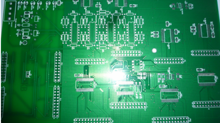
Green oil refers to the ink coated on the copper foil on the PCB. This layer of ink can cover unexpected conductors except for soldering pads. It can avoid soldering short circuits during use and prolong the life of the PCB. It is generally called solder mask. Or solder mask; colors include green, black, red, blue, yellow, white, matte color, etc. Most PCBs use green solder mask ink, which is usually called green oil.
The plane of the computer motherboard is a PCB (printed circuit board), generally a four-layer board or a six-layer board. Relatively speaking, in order to save costs, low-end motherboards are mostly four-layer boards: the main signal layer, ground layer, power layer, and secondary signal layer. The six-layer board adds an auxiliary power layer and a middle signal layer. Therefore, a six-layer PCB The motherboard is more resistant to electromagnetic interference, and the motherboard is more stable.