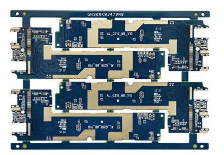
Most laptops pursuing light weight use flexible PCB substrates(FPC: Flexible Printed Circuit). Flexible PCB substrates are light, thin, and flexible. In addition to avoiding the internal batteries and hard disk drives of the laptop case In addition to other components, it also functions to connect to the motherboard, USB, LAN and other auxiliary PCB substrates (Sub Printed Circuit Board).
As the data transmission speed of notebook computers continues to increase, the sound waves that system manufacturers require flexible PCB substrates with high-speed transmission characteristics continue to increase. Therefore, the characteristic impedance value management of flexible PCB substrates must be carried out.
Flexible PCB substrates are divided into two categories: single-sided and double-sided. However, the signal layer and ground layer of flexible PCB substrates for notebook computers are mostly double-sided flexible PCB substrates composed of copper foil. The main reason is that the characteristic impedance value is different.

Management is easier, especially in the case of a single-sided flexible PCB substrate. Once the flexible PCB substrate comes into contact with the chassis, it is easily affected by the dielectric constant of the contacting object, causing the characteristic impedance to change. At this time, it is necessary to consider the surroundings of the flexible PCB substrate. Therefore, the management is more complicated than the double-sided flexible PCB substrate.
Then this article will discuss in depth the lightweight of flexible PCB substrates and the high-speed transmission technology that supports data transmission requirements.
Lightweight technology
The main method for the development of lightweight flexible PCB substrates is to greatly simplify the structure of double-sided flexible PCB substrates for traditional notebook computers. The specific method is to use conductive glue to make a ground layer on the surface of a single-sided flexible PCB substrate to form a pseudo-like double面结构. Surface structure.
The structure and characteristics of traditional double-sided flexible PCB substrates and lightweight flexible PCB substrates are compared at a glance. The specific contents are as follows:
Lightweight
In the case of a double-sided flexible PCB substrate, the signal layer and the ground layer are electrically connected by copper coating. Since the signal layer and the ground layer have copper foil coating as a whole, the copper content of the double-sided flexible PCB substrate is equivalent high.
In contrast to the light-weight flexible PCB substrate, the protective layer of the single-sided flexible PCB substrate is preliminarily set with openings filled with a large amount of conductive glue to form a ground layer, while the signal layer and the ground layer are electrically connected, so you can Effectively omit the copper coating which is very unfavorable in quality. In addition, the lightweight flexible PCB substrate can achieve the 50% weight reduction goal compared with the double-sided and double-sided flexible PCB substrate.
Thinning and flexibility
The lightweight flexible PCB substrate is basically a single-sided structure and does not require copper foil coating. Compared with the double-sided flexible PCB substrate, it can achieve 28% thinning effect, and its flexibility is better than that of the double-sided flexible PCB. The substrate is increased by 89%, so it is possible to make complex and fine avoiding curls inside the notebook computer chassis.
Transmission characteristics of lightweight FPC
Lightweight flexible PCB substrates have begun to be used in the parts of notebook computers that contact S-ATA1. (communication speed 1.5Gbit/s) with hard disk drives. At present, S-ATA1. is gradually being used by S-ATA 2 (communication speed 3.0Gbit/s). Instead, it is expected to evolve to S-ATA3 (communication speed 6.0Gbit/s) in the future. Therefore, lightweight flexible PCB substrates must be implemented to support the next generation of high-speed transmission.
The impedance characteristics of the lightweight flexible PCB substrate. The figure shows the impedance characteristics of the lightweight flexible PCB substrate. As the length of the transmission line increases slowly, the so-called transmission loss is finally formed.
The waveform simulation analysis result of the lightweight flexible PCB substrate shows that the eye pattern (Eye-pattern) does not touch the reference of S-ATA I, so the central hexagonal part forms a good waveform, compared with S- In the case of ATA2, the eye pattern has touched the central hexagonal part, and the symbol recognition margin is greatly reduced. This also proves that S-ATA1.'s highly acclaimed lightweight and flexible PCB substrate will be necessary when data transmission is speeded up in the future. Improve the transmission characteristics of the PCB substrate.