With the rapid development of electronic technology and the wide application of wireless communication technology in various fields, high-frequency, high-speed, high-density circuit board has gradually become one of the significant development trends of modern electronic products. High frequency and high-speed digitization of signal transmission force PCB to move towards micro hole and buried / blind hole, fine wire and uniform thin dielectric layer. High frequency and high-speed PCB design technology has become an important research field. This paper first makes a brief introduction to the high-frequency circuit board, then describes the PCB board design of high-frequency circuit board wiring skills, and finally introduces the PCB board design of high-frequency circuit board wiring precautions, specific follow the author to understand.
High frequency PCB board is a special circuit board with high electromagnetic frequency. Generally speaking, high frequency can be defined as the frequency above 1GHz. Its physical performance, accuracy and technical parameters are very high, and it is often used in automotive anti-collision system, satellite system, radio system and other fields. The high-frequency circuit board provided by the utility model is provided with a baffle which can block the flow of glue at the edge of the upper opening and the lower opening of the hollow groove of the core board, so that the flow of glue will not enter the hollow groove when the core board is bonded with the copper clad laminate placed on the upper surface and the lower surface, that is, the bonding operation can be completed by pressing once, which is better than the high-frequency circuit board which needs to be completed by pressing twice in the prior art, The high frequency circuit board in the utility model has the advantages of simple structure, low cost and easy manufacture.
1, The less lead bends between pins of high-speed electronic devices, the better
In high frequency circuit, it is better to use full straight line, which needs to be turned, and can be turned by 45 degree broken line or arc. This requirement is only used to improve the fixation strength of copper foil in low frequency circuit, but in high frequency circuit, meeting this requirement can reduce the external emission and mutual coupling of high frequency signal.
2, The less lead layer alternation between pins of high frequency circuit devices, the better
The so-called "less interlaminar alternation of leads, the better" means that the fewer vias used in the process of component connection, the better. One via can bring about 0.5pf distributed capacitance. Reducing the number of vias can significantly improve the speed and reduce the possibility of data error.
3, The shorter the lead between pins of high frequency circuit devices, the better
The radiation intensity of the signal is proportional to the length of the signal line. The longer the high-frequency signal lead is, the easier it is to couple to the components close to it. Therefore, for high-frequency signal lines such as signal clock, crystal oscillator, DDR data, LVDS line, USB line, HDMI line, the shorter the line is, the better.

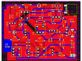
High frequency PCB circuit diagram
4, Pay attention to the "crosstalk" caused by the close parallel routing of signal lines(1) If parallel routing in the same layer is almost unavoidable, the directions of routing in two adjacent layers must be perpendicular to each other
PCB borad of high frequency circuit wiring should pay attention to the "crosstalk" caused by the close parallel routing of signal lines. Crosstalk refers to the coupling phenomenon between signal lines without direct connection. Because the high-frequency signal is transmitted in the form of electromagnetic wave along the transmission line, the signal line will act as an antenna, and the energy of electromagnetic field will be emitted around the transmission line. The unwanted noise signal between signals due to the mutual coupling of electromagnetic field is called crosstalk. The parameters of PCB board layer, the distance between signal lines, the electrical characteristics of driver and receiver, and the termination mode of signal line all have certain influence on crosstalk. Therefore, in order to reduce the crosstalk of high-frequency signals, the following points should be done as far as possible when wiring:
(1) If parallel routing in the same layer is almost unavoidable, the directions of routing in two adjacent layers must be perpendicular to each other;
(2) If the wiring space allows, inserting a ground wire or ground plane between two lines with serious crosstalk can play the role of isolation and reduce crosstalk;
(3) When there is time-varying electromagnetic field in the space around the signal line itself, if parallel distribution cannot be avoided, a large area of "ground" can be arranged on the opposite side of the parallel signal line to greatly reduce the interference;
(4) In the digital circuit, the clock signal is usually the signal with fast edge change, which causes great external crosstalk. Therefore, in the design, the clock line should be surrounded by ground wire, and more ground wire holes should be made to reduce the distributed capacitance, so as to reduce the crosstalk;
(5) For the high frequency signal clock, the low voltage differential clock signal parallel package ground mode should be used as far as possible, and the integrity of package ground drilling should be paid attention to;
(6) On the premise of wiring space permission, increase the distance between adjacent signal lines, reduce the parallel length of signal lines, and try to make the clock line perpendicular to the key signal line instead of parallel;
(7) The idle input terminal should not be suspended, but should be grounded or connected to the power supply (the power supply is also grounded in the high frequency signal circuit), because the suspended line may be equivalent to the transmitting antenna, and the grounding can suppress the transmission. It has been proved that this method can be used to eliminate the crosstalk.
5, High frequency decoupling capacitor is added to the power supply pin of integrated circuit block
A high frequency decoupling capacitor is added to the power pin of each IC block. Increasing the high-frequency decoupling capacitance of the power supply pin can effectively suppress the interference of high-frequency harmonics on the power supply pin.
6, PCB board ground wire of high frequency digital signal is isolated from the ground wire of analog signal
When connecting analog ground wire and digital ground wire to common ground wire, it is necessary to connect with high frequency choke magnetic beads or directly isolate and select suitable place for single point interconnection. The ground potential of the ground wire of high frequency digital signal is generally inconsistent, and there is a certain voltage difference between them. Moreover, the ground wire of high-frequency digital signal often has very rich harmonic components of high-frequency signal. When the ground wire of digital signal and analog signal is directly connected, the harmonic of high-frequency signal will interfere with the analog signal by coupling the ground wire. Therefore, in general, the ground wire of high-frequency digital signal and analog signal should be isolated, which can be connected by single point at the right position or by the way of high frequency choke magnetic beads.
7, PCB borad should avoid loops formed by routing
All kinds of high-frequency signal wiring should not form a loop as far as possible. If it cannot be avoided, the loop area should be as small as possible.

High frequency PCB circuit diagram
In conclusion, the birth of a circuit PCB board is from scratch, from simple to complex. If we use a fairy tale to describe it, it is the process of Cinderella from the cabin to the castle. It's a legendary and beautiful experience. Hope youcould leran more from this passage, and if you have any idea about PCB board, IPCB is glad to communicate with you!