One, the bill of materials
Insert or mount components in strict accordance with the bill of materials, PCB silk screen and outsourcing processing requirements. When the material does not match the bill, the PCB silk screen, or conflicts with the process requirements, or the requirements are vague and the operation cannot be performed, it should be timely Contact our company to confirm the correctness of materials and process requirements.
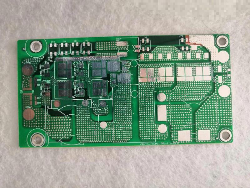
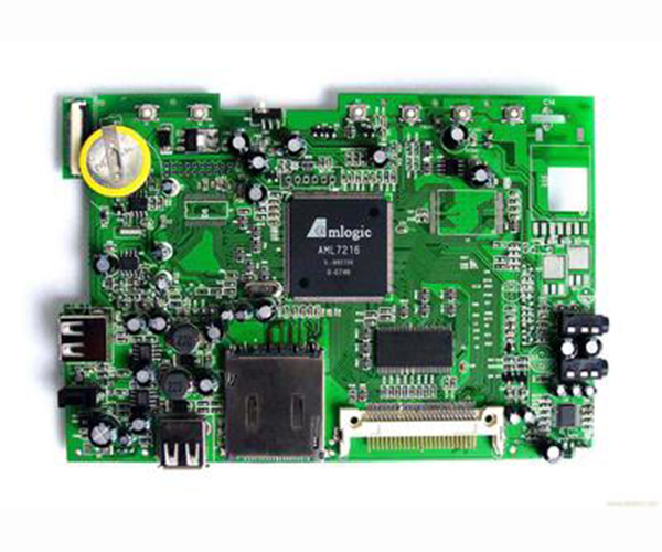
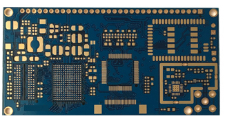
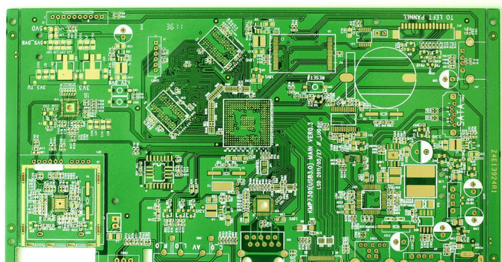
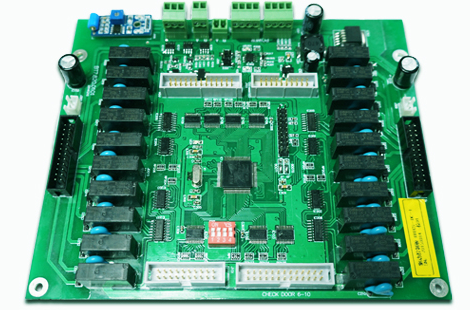
PCBA foundry material
2. Anti-static requirements
1. All components are treated as electrostatic sensitive devices.
2. All personnel who come into contact with components and products wear anti-static clothes, anti-static bracelets, and anti-static shoes.
3. During the raw materials entering the factory and in the warehouse, the electrostatic sensitive devices are all anti-static packaging.
4. During the operation, use an anti-static work surface, and use anti-static containers for the components and semi-finished products.
Anti-static requirements
5. The welding equipment is grounded reliably, and the electric soldering iron adopts anti-static type. All must be tested before use.
6. The semi-finished PCB board is stored and transported in an anti-static box, and the isolation material uses anti-static pearl cotton.
7. The whole machine without shell uses anti-static packaging bag.

Anti-static requirements for PCBA processing
Third, the provisions of the component appearance mark insertion direction
1. Polarity components are inserted according to polarity.
2. For components with silk-screened on the side (such as high-voltage ceramic capacitors) when inserted vertically, the silk screen faces right; when inserted horizontally, the silk screen faces down. When the components (not including the chip resistors) silk-printed on the top are inserted horizontally, the font direction is the same as the direction of the PCB screen printing; when inserted vertically, the upper side of the font faces right.
3. When the resistance is inserted horizontally, the error color ring faces to the right; when the resistance is inserted vertically, the error color ring faces down; when the resistance is inserted vertically, the error color ring faces the board.
Fourth, PCB welding requirements
1. The pin height of the plug-in component on the soldering surface is 1.5~2.0mm. SMD components should be flat against the board surface, and the solder joints should be smooth, without burrs, and slightly arc-shaped. The solder should exceed 2/3 of the height of the solder end, but should not exceed the height of the solder end. Less tin, ball-shaped solder joints, or solder-covered patches are all bad.
2. The height of the solder joints: the height of the solder climbing pins should not be less than 1mm for the single-sided board, and the double-sided board should not be less than 0.5mm, and the tin must be penetrated.
3. Solder joint shape: Conical shape and covering the entire pad.
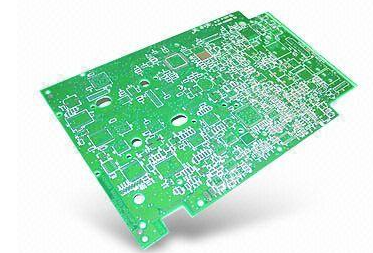
PCBA welding process
4. The surface of the solder joints: smooth, bright, no black spots, flux and other debris, no spikes, pits, pores, copper exposed and other defects.
5. Solder joint strength: fully wetted with pads and pins, no false soldering or false soldering.
6. Solder joint cross-section: the component's cutting foot should not be cut to the solder part as much as possible, and there should be no cracking on the contact surface between the lead and the solder. There are no spikes or barbs at the cross section.
7. Needle base welding: The needle base must be mounted on the bottom board, and the position is correct and the direction is correct. After the needle base is welded, the bottom floating height should not exceed 0.5mm, and the skew of the base body should not exceed the silk screen frame. The rows of needle holders should also be kept neat and not allowed to be misaligned or uneven.
Five, transportation
In order to prevent PCBA damage, the following packaging should be used during transportation:
1. Container: anti-static turnover box.
2. Isolation material: anti-static pearl cotton.
3. Placement spacing: there is a distance greater than 10mm between the PCB board and the board, and between the PCB board and the box.
4. Placement height: There is a space greater than 50mm from the top surface of the turnover box to ensure that the turnover box is not pressed against the power supply, especially the power supply of the wire.
Six, plate washing requirements
The board surface should be clean and free of tin beads, component pins, and stains. Especially at the solder joints on the plug-in surface, there should not be any dirt left by soldering. The following devices should be protected when washing the board: wires, connecting terminals, relays, switches, polyester capacitors and other easily corrosive devices, and the relays are strictly prohibited to be cleaned by ultrasonic.
Seven, all components are not allowed to go beyond the edge of the PCB board after installation.
8. When PCBA goes through the furnace, because the pins of the plug-in components are scoured by the tin flow, some plug-in components will be tilted after being soldered through the furnace, causing the body of the component to exceed the silk screen frame. Therefore, the repair soldering staff after the tin furnace is required to properly perform it. Fix.