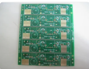
This example takes a four-layer computer motherboard as an example to describe in detail the entire process of PCB copying for this computer motherboard and its methods and skills for your reference.
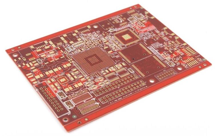
A four-layer computer motherboard with components that have not been disassembled. The board includes various chipsets, interfaces, socket expansion slots, and so on.
The specific implementation process is as follows:
(1) Preliminary preparations
1. Dismantle the board
First, use a digital camera to take two photos of the front and back sides of the four-layer computer motherboard. All the components in the photos are clearly identifiable to facilitate the later verification of the component positions. Use a small air gun to heat the component to be removed, clamp it with tweezers and let the pipe wind blow it away.

Disassemble the resistor first, then the capacitor, and finally the IC, and record the components that were dropped and previously installed reversely. Before disassembling, prepare a table with record items such as tag number, package, model, value, etc., paste double-sided tape on the component item of the component table, note the tag number, and paste the removed components one by one to the tag number Corresponding positions, after disassembling all the components, use the bridge to measure their values (some components will change their values under the action of high temperature, so the measurement should be performed after all the components have cooled down. At this time, the measured values More accurate), after the measurement is completed, enter the data into the computer for archiving.
2. Go to tin
Using flux, remove the remaining tin dross from the PCB surface where the components are removed with a tin suction wire, and adjust the temperature of the soldering iron appropriately according to the number of layers of the PCB. Since the multi-layer board heats up faster and is not easy to melt the tin, it should be Increase the temperature of the soldering iron, but not too high to avoid scalding the ink. Wash the tin-free board with washing water or alcohol and then dry it.
(2) Surface copy board
1. Scan the surface board
Use water gauze paper to lightly polish the upper and lower surfaces of the four-layer PCB bare board, and polish away the silk screen, ink and characters on the PCB surface to expose bright copper (there is a very important trick to polish the pads-the polishing direction must be It must be perpendicular to the scanning direction of the scanner). Then put the two layers of the surface into the scanner, start PHOTOSHOP, and scan the upper and lower layers of the circuit board in color. The PCB must be placed horizontally and straight in the scanner, otherwise the scanned image cannot be used.
2. Draw the surface layer PCB board
The first step is to adjust the contrast and brightness of the canvas in PHOTOSHOP, so that the part with copper film and the part without copper film have a strong contrast, and then turn the second image into black and white, and check whether the lines are clear. If not, repeat This step. If it is clear, save the picture as black and white BMP format files TOP1.BMP and BOT1.BMP.
The second step is to convert the two BMP format files to PROTEL format files, and transfer them into two layers in PROTEL. If the positions of the PAD and VIA on the two layers basically coincide, it indicates that the previous steps are well done. If there is Deviation, repeat the previous step.
The third step is to convert TOP1.BMP and BOT1.BMP into TOP1.PCB and BOT1.PCB respectively, pay attention to the conversion to the SILK layer, which is the yellow layer, and then trace on the TOP and BOT layers, and according to the scan Place the device on the drawing and delete the SILK layer after drawing.
The fourth step is to import TOP1.PCB and BOT1.PCB in PROTEL and combine them into one picture.
The fifth step is to use a laser printer to print the TOP LAYER and BOTTOM LAYER on the transparent film (1:1 ratio), put the film on the PCB, and compare whether there are errors. If they are correct, the top layer is completed. And the copy board on the bottom.