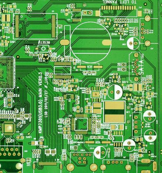
Computer-aided manufacturing (PCB design CAM) is to perform various process treatments according to the specified process. The various process requirements mentioned above must make necessary preparations before light painting. Such as mirroring, solder mask enlargement, process line, process frame, line width adjustment, center hole, outline line and other issues must be completed in the process of PCB design CAM. Special attention should be paid to the small spaces in the user files, which must be dealt with accordingly.
Because the process flow and technical level of each factory are different, in order to meet the final requirements of the user, necessary adjustments must be made in the production process to meet the user's requirements in various aspects such as accuracy. Therefore, PCB design CAM processing is an indispensable process in modern printed circuit manufacturing.
1. The work done by PCB design CAM

1. The size of the pad is revised, and the D code is combined.
2. Correction of line width, combined with D code.
3. Check the minimum spacing, between the pad and the pad, between the pad and the line, and between the line and the line.
4. Check the aperture size and combine them together.
5. Check the minimum line width.
6. Determine the expansion parameters of the solder mask.
7. Perform mirroring.,
8. Add various craft lines and craft frames.
9. Carry out line width correction to correct undercut.
10. Form the center hole.
10. Add the shape angle line.
6. Add positioning holes.
10. Imposition, rotation, mirroring.
10. Piece together.
10. Graph overlay processing, corner cutting and tangent processing.
10. Add user trademark.
2. The organization of PCB design CAM process
As there are dozens of popular CAD software on the market now, the management of CAD procedures must first be organized from the perspective of organization, and a good organization will achieve the effect of getting twice the result with half the effort. Since the Gerber data format has become a standard in the light painting industry, Gerber data should be used as the processing object in the entire light painting process. If CAD data is used as the object, the following problems will arise.
(1) There are too many types of CAD software. If various technological requirements must be completed in the CAD software, every operator is required to be proficient in the operation of each kind of CAD software. This will require a long training period to enable operators to become skilled workers and to meet actual production requirements. This is uneconomical from a time and economic point of view.
(2) Due to the numerous process requirements, some requirements cannot be achieved with certain CAD software. Because the CAD software is used for PCB design, it does not take into account the special requirements in the process, so it cannot meet all the requirements. The PCB design CAM software is specially used for process processing, and it is the best to do these tasks.
(3) PCB design CAM software has powerful functions, but it all operates on Getber files, not CAD files.
(4) If CAD is used for process processing, each operator is required to be equipped with all CAD software, and there are different process requirements for each kind of CAD software. This will cause unnecessary confusion to management.
In summary, the PCB design CAM organization should be the following structure (especially large and medium-sized enterprises).
1. All process processing is unified with Gerber data as the processing object.
2. Each operator must master the skills of converting CAD data into Gerber data.
3. Each operator must master one or several operating methods of PCB design CAM software.
4. Develop a unified process specification for Gerber data files.
5. PCB design CAM process can be handled by several operators in a relatively centralized manner for management.
A reasonable organization will greatly improve management efficiency, production efficiency, and effectively reduce the error rate, so as to achieve the effect of improving product quality.