In SMT patch processing, what customers value most is quality. Merchants can only make quality with their heart. When the quality is good, if the price is given an affordable price, then the two parties can cooperate for a long time. In addition, the personnel must be stable, and the front-line employees, technical and process engineers must be as stable as possible. The personnel in these key positions must be stable. Negotiations with customers must be done first, and try to operate according to the contract. Long-term cooperation!
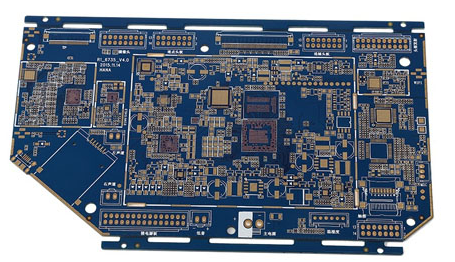
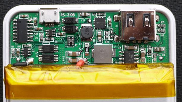
SMT chip processing technology
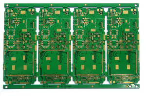
First of all, SMT processing double-sided mixing process:
1: Incoming inspection and repair => B-side repair adhesive of printed circuit board => SMD => curing => flap =>
PCB side A plug-in=>wave soldering=>cleaning=>testing=>rework
This SMT processing technology is suitable for use when large SMDs such as PLCC are mounted on both sides of the PCB.
2: Incoming inspection and repair => PCB's A-side plug-in (pin bend) => flip board => PCB's B side point
repair glue => patch => curing => flipping => wave soldering => cleaning => testing => repair
This SMT process is suitable for reflow soldering on the A side and wave soldering on the B side of the PCB. In the SMD assembled on the B side of the PCB, this process should be used when there are only SIT or SOIC (28) pins or less.
3: Incoming inspection and repair => PCB A-side silk screen solder paste => SMD => Drying => Reflow soldering => Plug-in, bent pins => Flip board => PCB SMT B edge patch glue => Paste Sheet => Curing => Turnover => Wave soldering => Cleaning => Testing => Rework
A-side mixed surface, B-side mounting.
4: Incoming maintenance => B pasta repair glue for printed circuit boards => SMD => curing => flipping => PCB A side silk screen solder paste => SMD =>

=>plug-in=>B surface wave=>cleaning=>detection=>rework A surface reflow
A-side mixed surface, B-side mounting, first two-sided mounting, reflow soldering, post-insertion, after wave soldering
5: Incoming inspection => PCB printed solder paste on the B side (point repair glue) => patch => drying (curing) => reflow soldering => flipping board =>
The solder paste silk screen of the PCB on the side of the PCB => SMD => Drying => Reflow soldering (local soldering can be used) => Plug-in => Wave soldering
(For example, plug in a small device, you can use manual soldering) => cleaning => testing => repair
Two, double-sided assembly;
1: Incoming inspection and repair => one side of the printed circuit board screen printed solder paste (repair glue) => patch => drying (curing) => one side reflow => cleaning => flipping => the second side of the PCB Screen printing solder paste (patch glue) => patch => drying => reflow soldering (b side only => cleaning => test => repair) The type used in this process in the PCB is PLCC SMD installation on both sides Use such a big one.
2: Incoming inspection and repair => one side of the printed circuit board printed solder paste (repair glue) => patch => drying (curing) => one side reflow => cleaning => flipping => PCB second pasta Repair glue=>SMD=>curing=>B-side wave soldering=>cleaning=>test=>rework) This type of reflow soldering PCB process of the A side, B side of the printed circuit board assembly patch, This technique should be used only when using SOT or SOIC (28) pins or less.
Third, single-sided assembly:
Incoming test => silk screen solder paste (point repair glue) => patch => drying (curing) => reflow soldering => cleaning => testing => repair
Four-sided mixing technology:
Incoming test => PCB printed solder paste on side A (point repair glue) => patch => drying (curing) => reflow soldering => cleaning => plug-in => wave soldering => cleaning => inspection => rework
SMT patch processing process precautions:
A. Conventional SMD placement
Features: SMT placement accuracy is not high, the number of components is small, and the component varieties are mainly resistors and capacitors, or there are individual special-shaped components.
Hub process: 1.Solder paste printing: FPC is positioned on a special pallet for printing by its appearance. Generally, small semi-automatic printing machine is used for printing, or manual printing can also be used, but the quality of manual printing is worse than semi-automatic printing.
2. SMT process placement: Generally, manual placement can be used, and individual components with higher position accuracy can also be placed by manual placement machine.
3. Welding: Reflow welding is generally used, and spot welding can also be used in special circumstances.
2. SMT processing in high-precision placement
Features: There must be a MARK mark for substrate positioning on the FPC, and the FPC itself must be flat. It is difficult to fix the FPC, and it is difficult to ensure consistency during mass production, and it requires high equipment. In addition, it is difficult to control the printing solder paste and placement process.
The key process: 1. FPC fixation: from the printing patch to the reflow soldering, the entire process is fixed on the pallet. The pallet used requires a small thermal expansion coefficient. There are two fixing methods, and the mounting accuracy is used when the QFP lead spacing is more than 0.65MM A; Method B is used when the placement accuracy is less than 0.65MM for QFP lead spacing.
Method A: The pallet is placed on the positioning template. The FPC is fixed on the pallet with a thin high-temperature resistant tape, and then the pallet is separated from the positioning template for printing. The high-temperature tape should have a moderate viscosity, and it must be easy to peel off after reflow soldering, and There is no residual glue on the FPC.
Method B: The pallet is customized, and its process requirements must be minimally deformed after multiple thermal shocks. The pallet is equipped with a T-shaped positioning pin, and the height of the pin is slightly higher than that of the FPC.
2. Solder paste printing: Since the pallet is loaded with FPC, there is a high-temperature resistant tape for positioning on the FPC, so that the height is inconsistent with the pallet plane, so an elastic squeegee must be selected when printing. The composition of the solder paste has a greater impact on the printing effect, and it is necessary Choose a suitable solder paste. In addition, the printing template of the B method needs to be specially processed.
3. Mounting equipment: First, the solder paste printing machine, the printing machine should have an optical positioning system, otherwise the welding quality will have a greater impact. Secondly, the FPC is fixed on the pallet, but the total distance between the FPC and the pallet There will be some tiny gaps, which is the biggest difference from the PCB substrate. Therefore, the setting of equipment parameters will have a greater impact on the printing effect, placement accuracy, and welding effect. Therefore, the FPC placement requires strict process control.