1. What problems should be paid attention to when using PCB components?
In the PCB circuit board proofing, the reasonable and effective use of components is an important guarantee for the stability and quality of the circuit board. So, what issues should be paid attention to when using components in the PCB proofing process?
1. Limit the output current to avoid the locking effect of the CMOS circuit: the locking effect means that there are parasitic PNP transistors and NPN transistors in the internal structure of the CMOS circuit, and they form a parasitic PNPN thyristor structure. . The common solution is to use a resistor to separate each output terminal from its cable, and use two high-speed switching diodes to clamp to VDD (drain power) and VSS (source power) with the cable. .
2. Use a filter network: Sometimes a long input cable is needed between the CMOS circuit system and the mechanical contacts, which increases the possibility of electromagnetic interference, so you should consider using a filter network.

3. Forming an RC network: For the sensitive input of a bipolar device, an RC network composed of a resistor with a larger resistance value and a capacitor of at least 100pF can be used to reduce the impact of electrostatic discharge.
4. Avoid floating of the input pins of CMOS devices: this is because once the input pins are floating, the input potential will be in an unstable state, which will not only destroy the normal logical relationship of the circuit, but also easily cause electrostatic breakdown and external noise interference. The redundant input terminal should be dealt with separately according to the function of the circuit.
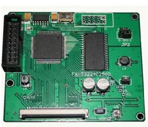
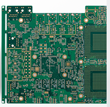
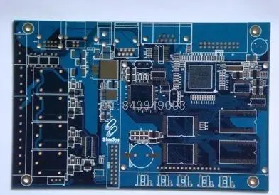
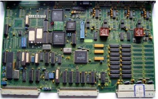
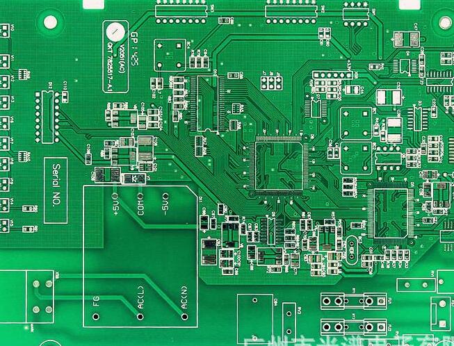
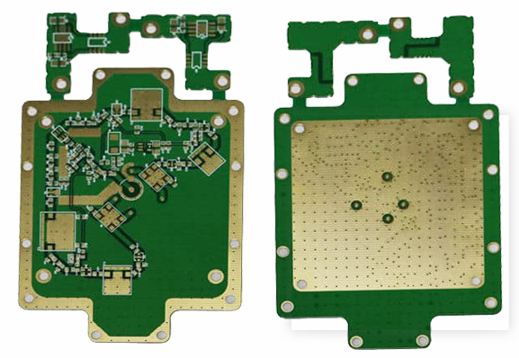
2. Simple maintenance skills and production process of circuit boards
The names of the circuit boards are: circuit boards, PCB boards, aluminum substrates, high frequency boards, thick copper boards, impedance boards, PCBs, ultra-thin circuit boards, ultra-thin circuit boards, printed (copper etching technology) circuit boards, etc.
Circuit board repair skills: observation method
This method is quite intuitive, through careful inspection, you can clearly see the burnt traces. When using this method, you need to pay attention to the following issues:
One step: Determine whether the circuit board is artificially damaged by observation, mainly by observing the following aspects:
(1) Whether the corners of the board are deformed; whether the chip is deformed, and whether other parts are deformed.
(2) Whether there are any signs of prying on the chip and socket.
(3) There is a problem with whether the circuit board chip is inserted. This is damaged when the power is turned on, so pay attention to it.
(4) Whether the corresponding short-circuit terminal of the circuit board is inserted wrongly or reversely.
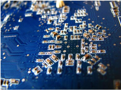
Step 2: Carefully observe the components related to this circuit board, every capacitor, resistor, etc. must be observed to see if there is any blackening. Since the resistance cannot be seen, it can only be measured with an instrument. Related bad parts should be replaced in time.
Three steps: Observe the circuit board integrated circuit, such as CPU, AD and other related chips, and make timely corrections when observing bulging, burning and other related conditions.