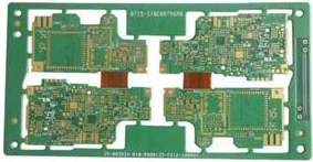
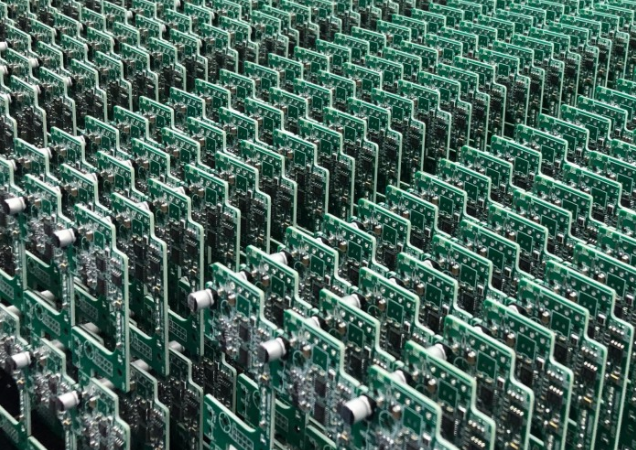
With the development of the PCB industry, smt chip processing has become more and more popular. This kind of processing technology has many characteristics, its products are small and have good high frequency, but it still has a lot of requirements for the production environment, temperature, cleanliness, etc. will have a certain impact on the product. When smt chip processing manufacturers are engaged in production and processing, some products will inevitably have flaws. Knowing empty soldering, bridging or wrong parts, etc., what are the reasons for these flaws?
1. Empty welding: There is no tin or other factors between the part pin or the lead pin and the tin pad.
2. False welding: The phenomenon of false welding is similar to that of empty welding, but the amount of tin in the tin pad is too small, which is lower than the standard of the joint surface.
3. Cold soldering: After the tin or solder paste is gasified in the return air furnace, there are still fuzzy granular attachments on the tin pad.
4. Bridging: The foot parts are short-circuited by the excess solder between the feet. Another phenomenon is caused by the improper operation of the inspectors using tweezers, bamboo skewers, etc., which causes the feet to touch and short-circuit, or scratch the CHIPS The pin causes residual tin dross to short-circuit the pin and the pin.
5. Wrong parts: If the specifications or types of the parts are not in conformity with the operation regulations or BOM, ECN, it is a wrong part.
6. Missing parts: The address of the parts should be placed, and there is a vacancy due to abnormality.
7. Polarity reversal: the correctness of the polarity orientation is not the same as the assembly of the processed engineering sample, that is, the polarity is wrong.
smt patch processing factory

8. Parts upside down: SMT parts must not be upside down, and CR has no specifications on the bottom because it is completely white, so it cannot be placed upside down even though it has no polarity.
9. Part offset: The offset between the welding point and the PAD position on the surface of all the parts of the SMT should not be greater than 1/2 area.
10. Tin pad damage: In the normal process, the pad (PAD) cannot be damaged when it is vaporized and welded by the return air furnace. The general reason for the damage of the solder pad is that the solder pad is damaged by improper use of soldering iron during repair. Those who can repair the normal shipment, the serious ones are included in the judgment of substandard products, or the transplantation is scrapped.
11. Pollution and uncleanness: Poor SMT processing operations, resulting in unclean board surface or foreign matter between the feet of CHIPS, or poor repair of CHIPS, a little glue, and anti-solder paint are regarded as unqualified products. However, repairs may be classified as substandard products depending on the circumstances.
12. SMT board burst: When the PCB board passes through the high temperature of the return air furnace, it is a defective product due to the poor material of the board itself or the abnormal temperature of the return air furnace.
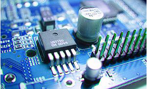
13. Overlay welding: there is too much solder in the solder joints, and the feet or outlines of the parts can not be seen.
The above are some undesirable phenomena and their reasons during the production and processing by smt chip processing manufacturers. In addition to these listed above, there are actually many other defects, such as scratches, kneeling, floating parts, etc. For these problems, smt chip processing manufacturers have also given corresponding countermeasures to reduce the possibility of occurrence.