PCB is a more important existence in today's electronic industry. After the design of the PCB patch is completed, if a more detailed inspection is not performed on it, it will be very troublesome if there is a problem in the future application, so the PCB is functional Inspection has become an indispensable step, which can provide greater assurance for subsequent production and ensure that no major mistakes will be caused due to temporary negligence. So what inspection items should be carried out after PCB design?
1. DFM review of the light board: Whether the light board production meets the process requirements of PCB manufacturing, including wire width, spacing, wiring, layout, vias, Mark, wave soldering component direction, etc.
2. Review the match between the actual components and the pads: whether the purchased actual SMT components and the designed pads are consistent (if inconsistencies are indicated with a red mark), and whether they meet the smaller spacing requirements of the placement machine.
3. Generate three-dimensional graphics: generate three-dimensional graphics, check whether the space components interfere with each other, whether the component layout is reasonable, whether it is conducive to heat dissipation, whether it is conducive to the heat absorption of SMT reflow welding, etc.
4. Optimization of PCBA production line: optimize placement sequence and material station location. Input the existing placement machine into the software, and allocate the components mounted on the existing board, how many types Siemens pastes, which locations, how many types around the world, which locations, which stations pick materials, etc., So as to optimize the SMT patch processing program and save time. For multi-line production, the placement of components can also be optimized.

5. Work instructions: automatically generate work instructions for workers on the production line.
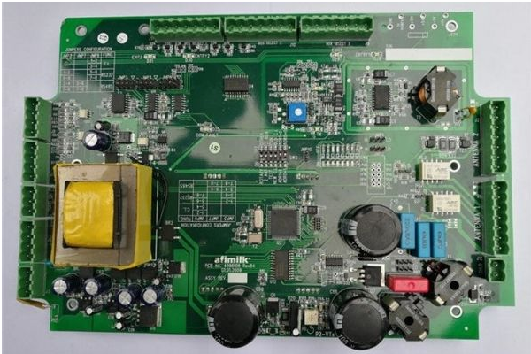
PCB patch
6. Revision of inspection rules: The inspection rules can be modified. If the component spacing is smaller than 0.1mm, it can be set to 0.2mm according to the specific model, manufacturer, and board complexity: the wire width is as small as 6mi, and it can be changed to 5mil for high-density design.
7. Support Panasonic, Fuji, Universal placement software: it can automatically generate placement software, saving programming time.
8. Automatically generate steel plate optimization graphics.
9. Automatically generate AOI and X-RAY programs.
10. Inspection report.
11. Support various software formats.
2. Review the BOM, modify the corresponding errors, such as the manufacturer's spelling errors, etc., and convert the BOM into the software format.
The above are some of the inspection items that need to be carried out after the PCB patch design. In fact, to make a simple analogy, these inspection processes are like the analysis and inspections that we all perform after completing the test papers, troubleshooting errors and making the answer sheets better. With the continuous development of the electronics industry, PCB, as the carrier and connector of electronic components, plays a decisive role, and it has the advantages of designability, assembly, maintainability, etc., which has become more and more popular. application.