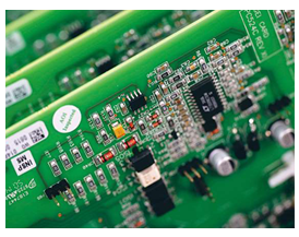
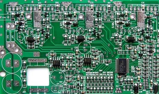
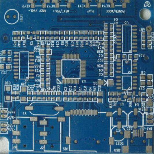
In the electronics industry, SMT chip processing mostly uses SMT processing, and there are many common faults during use. According to statistics, 60% of defects are caused by solder paste printing.
In the electronics industry, SMT chip processing mostly uses SMT processing, and there are many common faults during use. According to statistics, 60% of defects are caused by solder paste printing. Therefore, ensuring the high quality of solder paste printing is an important prerequisite for the quality of SMT patch processing. The following editor will show you how to solve printing errors during patching.
1. There is no gap between the stencil and the PCB printing method, that is, "touch printing". High stability requirements for all structures, suitable for printing high-precision solder paste. The metal screen is in good contact with the printed board, and is separated from the PCB after printing. Therefore, this method has high printing accuracy, and is especially suitable for fine-gap and super-macro printing.
1. Printing speed.
When the squeegee is pushed up, the solder paste rolls forward. Fast printing is good for stencils.

This kind of springback will also prevent the leakage of the solder paste, and the slurry cannot roll in the steel mesh, resulting in low resolution of the solder paste, which is the reason for the excessively fast printing speed.
The scale is 10*20mm/s.
2. Printing method:
Commonly used printing methods include touch printing and non-contact printing. The printing method for wire screen printing and printed circuit boards with blanks is "non-contact printing", which is generally 0.5*1.0mm, which is suitable for solder pastes of different viscosities. Use a scraper to push the solder paste into the stencil, open a hole and touch the PCB board. After the scraper is gradually removed, the stencil is separated from the PCB board, reducing the risk of vacuum leakage to the stencil.
3. Scraper type:
There are two types of scrapers: plastic scrapers and steel shovel. For ICs with a distance of no more than 0.5mm, steel solder paste can be selected to facilitate the formation of solder paste after printing.
4. Scraper adjustment.
In the welding process, the squeegee operating point is printed along the 45° direction, which can significantly improve the unevenness of the solder paste opening and reduce the damage of the thin steel plate with the opening. The pressure of the scraper is generally 30N/mm.
Solutions to printing failures in SMT patch processing
2. When installing, choose an IC mounting height with a spacing of no more than 0.5mm, 0mm, or 0~-0.1mm mounting height to avoid solder paste collapse due to too low mounting height and short circuit during reflow.
3. Remelting welding.
The main reasons for assembly failure caused by reflow welding are as follows:
a. Heating up too fast;
b. Overheating temperature;
c. The solder paste heating speed is faster than the circuit board heating speed;
d. The water flow is too large.
Therefore, when determining the remelting welding process parameters, all factors should be fully considered to ensure that there is no problem with the welding quality before the mass SMT patch assembly.