As an electronic engineer designing a circuit is a necessary hard work, but no matter how perfect the principle design is, if the circuit board design is unreasonable, the performance will be greatly reduced, and it may even not work properly in severe cases. According to my experience, I have summarized the following points that should be paid attention to in the PCB design, and I hope it can be enlightened to you.
No matter what software is used, there is a general procedure for PCB design, which will save time and effort in order, so I will introduce it according to the production process. (Because the protel interface style is similar to the windows window, the operating habits are also similar, and there is a powerful simulation function, and there are more people who use it. This software will be used as an explanation.)
Schematic design is the preliminary work. It is often seen that beginners just go to draw PCB boards in order to save trouble. This will outweigh the gains. For simple boards, if you are proficient in the process, you can skip it. But for beginners, you must follow the process, so that on the one hand, you can develop good habits, and on the other hand, the only way to avoid mistakes for complex circuits.
When drawing a schematic diagram, pay attention to the final connection of each file into a whole when designing the hierarchy, which is also of great significance for future work. Due to differences in software, some software may appear to be connected but not connected (in terms of electrical performance). If you don’t use related testing tools, in case something goes wrong, it’s too late to find out when the board is ready. Therefore, the importance of doing things in order has been repeatedly emphasized, and I hope to attract everyone's attention.

The schematic diagram is based on the designed project, as long as the electrical connection is correct, there is nothing to say. Below we focus on the problems in the specific board-making procedures.
1. Make a physical border
The closed physical frame is a basic platform for the future component layout and wiring, and it also plays a constraining effect on the automatic layout. Otherwise, the components coming from the schematic will be at a loss. But you must pay attention to accuracy here, otherwise installation problems in the future may be troublesome. In addition, it is best to use arcs at the corners. On the one hand, it can avoid sharp corners from scratching workers, and at the same time, it can reduce the effect of stress. In the past, one of my products always had the PCB board of the face shell broken during the transportation process, and it was just fine after switching to the arc.
2. Introduction of components and networks
It should be very simple to draw the components and the network in the frame, but there are often problems here. You must carefully solve the errors one by one according to the prompts. Otherwise, it will take more effort. The problems here are generally as follows:
The package form of the component can not be found, the component network problem, there are unused components or pins, these problems can be solved quickly by comparison.
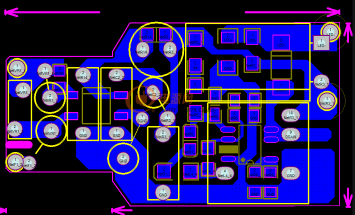
3. Component layout
The layout and wiring of the components have a great impact on the life, stability, and electromagnetic compatibility of the product, so special attention should be paid. Generally speaking, there should be the following principles:
(1) Placement order
First place the components related to the structure at a fixed position, such as power sockets, indicator lights, switches, connectors, etc. After these devices are placed, use the lock function of the software to lock them so that they will not be moved by mistake in the future. Then place special components and large components on the circuit, such as heating components, transformers, ICs, etc. Finally, place the small device.
(2) Pay attention to heat dissipation
The component layout should pay special attention to heat dissipation. For high-power circuits, the heating elements such as power tubes, transformers, etc. should be placed as close to the side as possible to facilitate heat dissipation. Do not concentrate in one place, and do not have high capacitors too close to avoid premature aging of the electrolyte.
4. wiring
PCB wiring principle
The knowledge of routing is very advanced, everyone will have their own experience, but there are still some common principles.
◆High-frequency digital circuit traces should be thinner and shorter
◆Attention should be paid to isolation between high current signal, high voltage signal and small signal (the isolation distance is related to the withstand voltage to be withstood. Normally, the distance between the board should be 2mm at 2KV, and it should be increased in proportion to this. For example, to withstand the 3KV withstand voltage test, the distance between the high and low voltage lines should be more than 3.5mm. In many cases, to avoid creepage, slots are also slotted between the high and low voltages on the printed circuit board.)
5. Adjust and perfect
After completing the wiring, all you need to do is to adjust the text, individual components, wiring, and apply copper (this work should not be too early, otherwise it will affect the speed and bring trouble to the wiring), also for the convenience of production, Commissioning and maintenance.
Copper coating usually refers to filling the blank area left by the wiring with a large area of copper foil. It can be covered with GND copper foil or VCC copper foil. To increase the conduction area of the power supply, to withstand a larger current before connecting to VCC). Grounding usually refers to wrapping a bunch of signal wires with special requirements with two ground wires (TRAC) to prevent it from being interfered by or interfered with by others. If you use copper instead of the ground wire, you must pay attention to whether the entire ground is connected, the current size, flow direction, and whether there are special requirements to ensure that unnecessary errors are reduced.
6. Check network
Sometimes the network relationship of the board drawn is different from the schematic diagram due to misoperation or negligence. At this time, it is necessary to check and verify. So don’t rush to hand it over to the plate maker after finishing the drawing, you should check it first, and then do the follow-up work.
7. Use simulation function
After completing these tasks, PCB software simulation can be carried out if time permits. Especially for high-frequency digital circuits, some problems can be found in advance, which greatly reduces the amount of debugging work in the future.