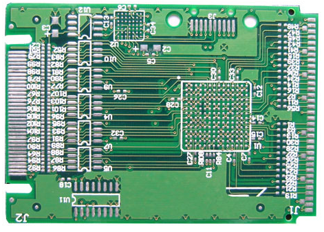
High-density interconnection (HDI) is a technology that is rapidly popularized in PCB design and integrated into various electronic products. HDI is a technology that provides a denser structure on the board by placing smaller components closer together, which also results in shorter paths between components.
HDI PCB is looking to enter more and more products:
Aerospace-smaller space requirements and lighter weight are ideal for this type of application
Computers and smartphones-Mobile phones and computers are taking full advantage of smaller form factors, reducing weight and increasing functionality, through integrated HDI circuits.
Medical equipment-Diagnosis and monitoring equipment becomes more reliable and expands with technical features that can help medical teams in patient treatment, supported by HDI PCB and advanced software.
Benefits of HDI
The HDI board utilizes buried or blind vias, or a combination, can also contain trace amounts of ovias with incredibly small diameters. This helps to combine more technology in less space while reducing the number of layers. Multi-layer HDI boards are also commonly used, using blind, buried, stacked and staggered vias to accommodate multiple layers through various construction methods.

With smaller components and blind via and pad technology, components can be placed closer together, resulting in faster signal transmission rates, while also reducing cross delay and signal loss. These are the key factors to improve the performance of HDI PCB board.
HDI boards are suitable for applications in terms of space, performance, reliability and weight. This makes them more suitable for almost all applications related to electronics, consumer products, computers and aviation.
Multi-layer HDI boards can provide a powerful interconnection of stacked vias, thereby achieving a high level of reliability, even in more extreme environments.
Disadvantages and precautions of HDI
Although the advantages of HDI are obvious, the technology also has shortcomings.
The equipment required for professional processing and manufacturing of HDI boards is expensive. Such equipment includes laser drills, laser direct imaging processes and other specialized manufacturing equipment and materials. This need for specialized equipment and operator training is partly responsible for the high cost of HDI manufacturing.
Attention to detail is essential to the design and manufacture of HDI printed circuit boards. This requires professional knowledge and experience.
Many PCB manufacturers have not yet invested or transitioned to laser direct imaging (LDI) for circuit board manufacturing. For HDI boards, tighter tolerances for finer lines and tighter spacing make LDI an important consideration for quality results. Although contact imaging is still widely used in PCB manufacturing, HDI is more suitable for HDI boards, although the cost of the equipment can be considerable.
Design and manufacture HDI PCB
PCBs designed for HDI applications require specific tools, as does the manufacturing process. The use of computer-aided design (CAD) software for design and computer-aided manufacturing (CAM) tools is considered a necessary condition for the use of HDI technology for PCB creation.