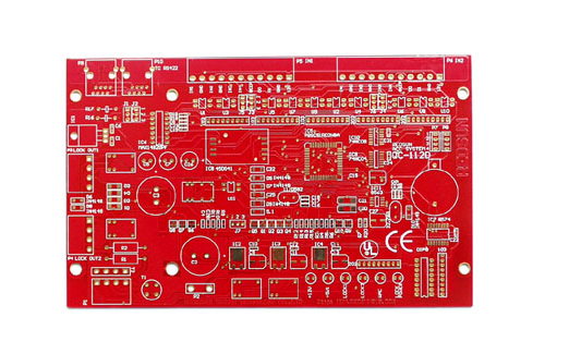
The primary considerations in PCB layout are size and shape. The final result must be adapted to the environment in which the circuit board is installed and used, thereby driving the design process. Space considerations may require the use of multi-layer or high-density interconnect (HDI) designs. Some projects require special board shape and weight restrictions, making the layout particularly challenging.
Although this may not be the main consideration when designing the initial circuit function, in the case of prototyping, etc., it will become higher and prioritized when laying out PCBs for manufacturing.
Consider the PCB manufacturer during the PCB layout stage. Not all manufacturers can produce higher numbers of multilayer boards or HDI PCBs. In most cases, PCB layout design that requires flexible or flexible rigid structure technology needs to be reviewed with the recommended supplier to ensure that the layout design and material requirements are met.
Special requirements such as the need to adopt lead-free structures or otherwise avoid potentially hazardous materials may be key points in making layout and construction decisions.
Technical PCB layout issues
Other more technical factors are considered in the PCB layout:
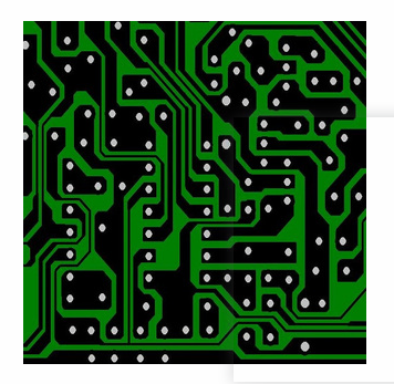
Trace width
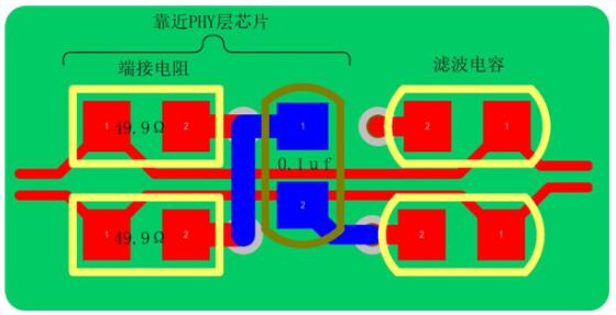
Spacing between traces
Tolerance of electrical factors that may affect the function of the circuit board
Clear the traces and components on the edge of the trace

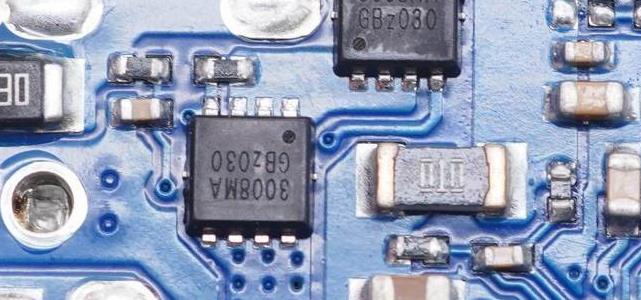
Component availability-components that are difficult to find or dedicated can significantly increase the cost of the final circuit board. If lower-cost alternatives can be produced, then a large number of circuit boards are expected to be produced, which may be a major problem.
Construction method-PCB layout largely depends on the physical structure of the circuit board: through-hole assembly, surface mount technology (SMT) or a combination of both. In recent years, the design of multi-layer and HDI boards has developed rapidly, and there are many specific layout requirements for these technologies.
The importance of PCB layout
The lack of efficient and accurate layout can cause almost unlimited problems, including:
Electromagnetic interference from conflicting components or trace placement
Conflict of components on both sides of the board
Designer's rework and manufacturing delays
Limited board functions
The board always fails
Solve many PCB layout problems
Now most PCB designers and manufacturers can use complex computer-aided design (CAD) and computer-aided manufacturing (CAM) software systems. These professional programs have many advantages over traditional engineering methods:
Drag and drop design-place components easily and accurately, and then let the software generate traces of connections. Move or add components quickly and easily.
Layout verification-Tolerance, compatibility, component placement, etc. are verified during design and before the PCB is released for manufacturing, even prototypes.
Reuse-Once the layout is approved and saved, it can be reused as a template for new PCB projects and used by other engineers.
Efficiency-Using these professional programs can speed up development, reduce errors, and speed up time to market.
Cost saving-efficiency is equivalent to saving redesign or manufacturing errors.
Error detection-catch basic errors in real time to avoid defects in manufacturing or delays detected by the manufacturer.
Rule creation-Many of these programs support the creation of custom rule sets specific to the designer's purpose. Creating these rules and storing them allows designers to share and enhance the functionality of the software.