1. The PCB design should be carried out in a certain order, such as from left to right and from top to bottom.
2. The wiring strip width and line spacing should be moderate, and the spacing between two pads of capacitor should be consistent with the spacing between capacitor lead pins as far as possible.
3. When designing the wiring diagram, the wiring should be as little as possible, and the lines should be simple and clear.
4. When designing the wiring diagram, pay attention to the arrangement sequence of pins and reasonable spacing between components.

5. Wiring direction:
Look from the surface of welding, the arrangement of components bearing as far as possible to keep consistent with schematic diagram, wiring direction is consistent with the circuit diagram line direction, because of the production process often need to test the various parameters on surface of the welding, so do check in for production, debug and repair (note: refers to the circuit performance and under the premise of the machine installation and panel layout requirements).
6. On the premise of ensuring the performance requirements of the circuit, the design should strive for reasonable wiring, less use of external connections across the line, and according to a certain charging requirements of wiring, intuitive, easy to install, height and maintenance.
7. The arrangement and distribution of each component should be reasonable and uniform, and strive to be neat, beautiful and strict in structure.
8. Layout direction of inlet and outlet terminals
(1) The two leads associated with the end of the distance is not too large, generally 2 -- 3/10 inches or so is appropriate.
(2) Incoming and outgoing lines should be concentrated on 1 to 2 sides as far as possible, and should not be too discrete.
9 potentiometer: IC seat placement principle
(1) potentiometer: used to adjust the output voltage in the voltage regulator, so the design potentiometer should be full in clockwise adjustment of the output voltage rise, counterclockwise regulator section output voltage reduction; In the adjustable constant current charger potentiometer used to adjust the charging current fold size, design potentiometer should be full in the clockwise adjustment, the current increases. The potentiometer should be placed in full machine structure installation and panel layout requirements, so should be as far as possible on the edge of the plate, rotating handle outward.
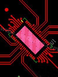
(2)IC seat: design printing board, in the use of IC seat under the occasion, we must pay special attention to the POSITION of the POSITIONING slot on the IC seat is correct, and pay attention to each IC foot position is correct, such as the first foot can only be located in the lower right corner line or the upper left corner of the IC seat, and close to the positioning slot (from the welding surface).
10. Position direction of resistor and diode in PCB layout:
PCB design is divided into two types: horizontal and vertical:
(1) flat: when the number of circuit components is not much, and the size of the circuit board is large, it is generally better to use flat; For the resistance below 1/4W flat, the distance between the two pads is generally 4/10 inches, 1/2W resistance flat, the distance between the two pads is generally 5/10 inches; Diode flat, 1N400X series rectifier, generally take 3/10 inches; 1N540X series rectifier tube, generally take 4 -- 5/10 inches.
(2) vertical: when the number of circuit elements is more, and the size of the circuit board is not large, the general PCB design is to use vertical, vertical when the distance between the two pads is generally 1-2/10 inches