Regarding the accuracy of reducing the influence of moisture on any type of printed circuit board. From material fusion, PCB layout, prototyping, PCB engineering, assembly to packaging and order delivery stages, attention should be paid to the influence of moisture in PCB manufacturing to avoid damage and other problems with PCB functions. In addition, let us have an in-depth understanding of the important measures to control humidity levels during the lamination process, the controls implemented during PCB assembly and control storage, packaging and transportation.
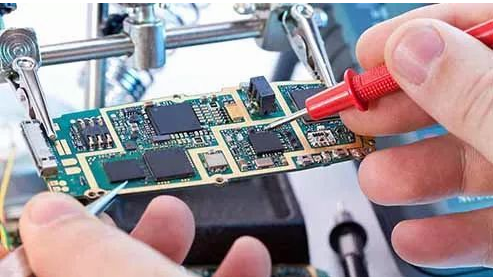
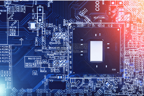
What are the factors that have a huge impact on the PCB assembly mechanism
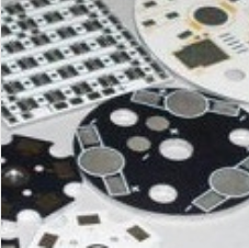
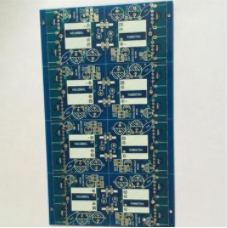
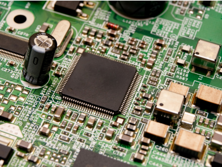
Rigid/flexible printed circuit board assemblies, cable bundles, boxed assemblies or wire harness PCB assemblies are made of various types of materials, which fully comply with the attributes required for strong mechanical and electrical performance in electronic products used in all major industries around the world . It needs high frequency, low impedance, compactness, durability, high tensile strength, low weight, multi-function, temperature control or humidity resistance, PCB is divided into single layer, double layer or multilayer, depending on the complexity of the circuit. Among all the serious problems that should be paid attention to in the initial stage of PCB manufacturing, humidity or humidity is the main factor that creates space for electronic and mechanical failures in PCB operations.
How does moisture cause huge troubles on printed circuit boards?
By being present in the epoxy glass prepreg, it diffuses in the PCB during storage, and when absorbed, moisture can form various defects in the PCB assembly. The wet process time in the PCB manufacturing process exists in micro cracks or can form a home in the resin interface. Due to the high temperature and vapor pressure parallel to the lead-free mechanism in PCB assembly, it will cause moisture absorption.

As adhesives and cohesive failures in printed circuit boards lead to delamination or cracking, moisture can make metal migration possible, resulting in a low impedance path for dimensional stability changes. With the decrease of the glass transition temperature, the increase of the dielectric constant and other technical damages, it will cause the circuit switching speed to decrease and the propagation time delay to be high.
The main effect of moisture in PCB is that it reduces the quality of metallization, lamination, solder mask and PCB manufacturing process. Due to the influence of moisture, the limit of thermal stress becomes excessive as the glass transition temperature decreases. Sometimes it can cause a severe short circuit, causing moisture to enter, leading to ion corrosion. Other common properties of moisture absorption in printed circuit board assemblies include flame retardancy or delamination, increased (DF) dissipation factor and (DK) dielectric constant, thermal stress on plated through holes, and copper oxidation.
Methods to reduce moisture in PCB manufacturing:
Regardless of whether simple or complex technologies are used in PCB manufacturing, there are many operations in PCB engineering that require wet processes and removal of residual moisture. The raw materials used in PCB manufacturing need to be protected during storage, handling, and stress during PCB assembly. The following is a short guide for implementing controls at various stages of PCB operation:
1. laminated
Lamination is a dehydration step in PCB manufacturing because the core and prepreg are stacked together to bond the layers into the laminate. The main factors that are controlled during the lamination process are temperature, time used and heating rate. Sometimes when the dryness is low, measures are taken to lower the vacuum to reduce the possibility of attracting internal voids for moisture absorption. Therefore, the use of gloves when handling prepregs can well control the level of moisture. This reduces cross-contamination. The non-corrosive humidity indicator card should be flexible to account for humidity levels when needed. Laminates should have a short washing cycle and be stored effectively in a controlled environment, which helps prevent moisture pockets from forming in the laminate.
2. Post lamination process and PCB assembly
After drilling in PCB manufacturing, photographic imaging and etching operations, the moisture absorption rate captured in the wet process is higher. Screen printing curing and solder mask baking are processed steps to relieve entrained moisture. By minimizing the holding time interval between steps and even keen to manage storage conditions, this is more effective in reducing the level of moisture absorption. By ensuring the early stages of PCB lamination, the circuit board is dry enough to help reduce the baking operation after lamination. In addition, high-quality surface treatment is used to prevent cracks during the drilling process, and the humidity of the residue is removed by baking before the hot-air solder leveling process. The baking time should be maintained by considering the decision level of moisture content, the complexity of PCB manufacturing, PCB surface treatment and sufficient thickness required for the circuit board.
Therefore, it is important to understand the latest situation of the effect of moisture in PCB manufacturing to avoid failures, damages and short circuits on the PCB, while increasing the cost of rework. Now, researchers are about to launch more advanced solutions, by using environmentally friendly PCB technology to control the moisture element in each step of PCB manufacturing, thereby saving time, energy and costs.