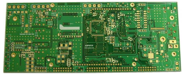
The systematic approach of the Design Rule Checker (DRC) is used in PCB design. After capturing the PCB design in the PCB schematic tool, DRC must be run to find violations of the design rules. This must be done before the back-end processing starts. Usually, the suppliers of schematic tools provide DRC, and most designers just use it.
However, vendor tools are universal and may not always be flexible enough to handle certain unique requirements. It is possible to send a request for a new function to be added to the DRC to the supplier, but this will cost money and time, especially if this operation must be performed multiple times. Fortunately, most tool vendors provide easy-to-use mechanisms, and you can write your own DRC to better meet your unique needs. Unfortunately, this powerful tool has not been widely recognized or utilized.
Because DRC must traverse the entire schematic diagram of the PCB design, including each symbol, each pin, and each network, if necessary, it can generate an unlimited number of useful "by-products" for each attribute. As explained in Section 4.0, they can well mark subtle design rule violations. For example, a by-product file may contain all decoupling capacitors in the design. If the number is much smaller or larger than expected, this may trigger a red flag of possible power line dv/dt problems [1]. These by-product files may be very needed, but they are definitely not generated by any commercial DRC.
Another benefit of this DRC is that it can be easily and quickly updated to accommodate new design features, such as new attributes that affect design rules. In addition, once you have gained enough experience in this field, many other possibilities will emerge.
For example, if you can write your own DRC, you can of course write your own bill of materials (BOM) generation tool, which can better handle certain unique requirements, such as where to obtain components that are not part of the schematic database "extra hardware" (Socket, heat sink or screw). Or you can write your own Verilog netlister, which is flexible enough to suit your design environment, such as where to obtain Verilog models or timing files for certain unique components. In fact, when DRC traverses the design schematic, it can collect all the necessary information to output the Verilog netlist for simulation and/or the BOM for PCB manufacturing.
It will be difficult to discuss these topics without providing some programming code. For this, we need to use the schematic capture tool as an example. In this article, we use ViewDraw from Mentor Graphics, which is part of the PADS-Designer product family. In addition, we use ViewBase, which is just a library of C routines that can be called to access the ViewDraw database. Using ViewBase, you can easily write a complete and useful DRC for ViewDraw in C/C++[2][3]. Please note that the principles we discuss here apply to any other PCB schematic tools.

In addition to the schematic database, DRC also needs some input files to tell it how to handle certain situations, such as the legal power net name that is automatically connected to the power plane. For example, if the power network is called POWER, it will be automatically connected to the power plane through a back-end packaging utility, such as ViewDraw's PCBfwd. The following is a list of these input files. These files should be placed in a fixed global location so that DRC can automatically find/read them at runtime and store information internally.
You can choose to create a file named legal_pwr_net_name that contains all the legal network names of the POWER signal, such as VCC, V3_3P, VDD. Please note that letter case may be important for some PCB layout/wiring tools, and usually VCC is different from Vcc or vcc. VCC can be a 5.0V power supply, and V3_3P can be a 3.3V power supply.
legal_pwr_net_name is optional, because the configuration file of the back-end packaging utility must usually contain a list of legal power/ground network names. If Allegro from Cadence Design Systems is the placement/layout tool, the file is named allegro.cfg for PCBfwd and it must have the following entries:
Ground VSS CGND GND GROUND
Power supply VCC VDD VEE V3_3P V2_5P + 5V + 12V
If DRC can directly read allegro.cfg instead of legal_pwr_net_name, it would be better (the possibility of introducing errors is less).
Normally, power/ground pins do not appear on component symbols. Instead, the symbol has an attribute (can be called SIGNAL) that specifies which pin is power or ground, and specifies the name of the network to which the pin should be connected:
SIGNAL = VCC: 10
SIGNAL = GROUND: 20
DRC can read this attribute and ensure that the network name is the name in the legal_pwr_net_name file. If not, the power pin will not be connected to the power plane, which is a very serious error.
Certain symbols must have power/ground pins because they are not connected to the normal power/ground plane. For example, the VCC pin of an ECL device can be connected to VCC or GROUND; its VEE pin can be connected to the GROUND or -5.0V plane. In addition, the power/ground pin can be connected to the filter first before entering the power/ground plane.
The network between this pin and the filter can have any name, and DRC will not be able to check this information. DRC can report this as an error, and the user must filter it out, or add the net name to the legal_pwr_net_name file just for this design. This is one reason why files such as legal_pwr_net_name may be needed. Finally, legal_pwr_net_name will be read by DRC 1) find the pull-up resistor, 2) check the letter case of the POWER net name in the PCB design, and 3) detect any unused pins directly connected to POWER.