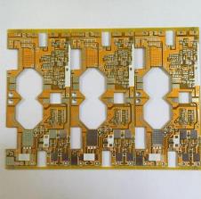
SMT assemblies are becoming more and more complex. Although SMT assembly manufacturers strive for 100% output, the reality is that it is very difficult to achieve. Although most electronic products currently use SMT components, the reduction in component size makes it very difficult to put them on the PCB. In addition, there are many other shortcomings of SMT components that need to be overcome, including:
What are the challenges faced by PCB manufacturers when building lead-free SMT components
Poor solder paste release
The solder paste release, in turn, is determined by the aspect ratio and the surface area ratio. The aspect ratio compares the minimum size of the template aperture with the template foil thickness. Aspect ratios below 1.5 are unacceptable. The surface area ratio compares the surface area of the template pores with the surface area of the template pore walls.

The lowest acceptable surface area ratio is 0.66. Although the aspect ratio and surface area ratio help predict solder paste release, it is also important to bond the solder paste to the SMT pad, and the size of the SMT pad depends on the size of the SMT pad. The difference in surface finish will in turn affect the size of the SMT pad. In order to be able to accurately predict the release of solder paste, an improved surface area ratio formula must be considered, which takes into account the change in the size of the SMT pad due to copper weight and surface finish. As smaller components become more mainstream, this becomes increasingly important. Generally, the bottom of the SMT pad matches the size in the electronic PCB file, while the top is smaller. When calculating the surface area ratio of the template, it is necessary to consider this smaller size of the top, because the smaller size of the top has a smaller surface area.
Bridging when printing
In addition to affecting solder paste release, copper weight and surface finish also affect bridging. Heavy copper weight or uneven surface finish will reduce the sealing performance between the PCB and the template. This can in turn allow the solder paste to squeeze out during printing and also cause bridging during printing. The sealing depends on the size of the SMT pad and the template hole. A template hole larger than the SMT pad will cause the solder paste to squeeze out between the PCB and the template.
In order to avoid this problem, it is necessary to reduce the width of the template aperture. This is especially true for heavy copper weight and uneven PCB surface treatment. This in turn ensures the possibility of solder paste extruding between PCB and PCB. The template is minimized.
Insufficient volume of SMT reflow solder
Although this is a common defect, the optical inspection can usually only be captured in a visual or automated process at the end of the SMT process. DFM review can sometimes also capture shortfalls before production. In order to overcome this problem, the required volume increase is based on the difference in size between leadless terminals and PCB pads. In addition, in the case of leadless components, an additional volume of solder paste needs to be printed on the toe side. It is also necessary to avoid increasing the width of the template aperture. Also need to pay attention to the thickness of the template foil. If the thickness of the foil needs to be adjusted to suit the SMT component, the aperture of the template also needs to be increased.
SMT reflux bridge
Due to the extrusion of the solder paste between the PCB and the PCB, the SMT reflow bridges multiple times. The template in printing, in other cases, it is due to PCB manufacturing problems, placement pressure, reflow settings, etc. due to SMT reflow soldering will also occur due to gull-wing packaging, because their component leads are exposed to heating. On the other hand, lead-free packages have uniform heating. The gull-wing package also has a limited surface area to wet the solder. If there is too much solder, the excess solder will overflow onto the PCB pads. However, the reduction in solder paste volume should always be focused on the gull-wing feet rather than the PCB pads. Although for most components, the volume reduction will be greatly reduced, care needs to be taken when the PCB surface finish is OSP and the solder is lead-free. In the case of lead-free solder, reducing the volume will expose the OSP after reflow. The exposed OSP in turn can cause many problems that affect reliability.
Although some SMT defects are limited to specific assembly lines or specific locations, many other SMT defects such as solder paste release, printing bridging, bridging of SMT Reflow, insufficient amount of solder on SMT Reflow and more of the above mentioned are universal. It is not limited to a specific set of variables. Therefore, it is necessary to pay close attention to their influence to ensure the reliability of operation.