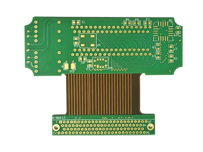
Common specifications for PCB drawing, PCB contains four files: schematic diagram, schematic library, package library file, PCB file
First create a new PCB project: File->New->Project->PCBProject
1. Schematic file name.SchDoc: File->new->Schmatic
2. Schematic library file name.SchLib: File->New->Library->Schematic Library
3. Package library file name.PCBLib: File->New->Library->PCB Library
4. PCB file name.PCBDoc: File->New->PCB
PCB common units
1mil = 0.0254mm
100mil = 2.54mm
1inch = 1000mil = 25.4mm
The typical via sizes used in PCB design and production are as follows:
The size of the via hole used for grounding or other special needs on the PCB is: the hole diameter is 16mil, the pad diameter is 32mil, and the anti-pad diameter is 48mil;
The size of the via hole used when the board density is not high is: the hole diameter is 12mil, the pad diameter is 25mil, and the anti-pad diameter is 37mil;
The size of the via hole used when the board density is high is: the hole diameter is 10mil, the pad diameter is 22mil or 20mil, and the anti-pad diameter is 34mil or 32mil;
The via size used under 0.8mm BGA is: hole diameter 8mil, pad diameter 18mil, anti-pad diameter 30mil.

The spacing of circuit lines is generally not less than 6mil
The distance between copper and copper is generally set to 20mil
The distance between copper skin and trace, copper skin and via (via) is generally 10mil
Power cord generally choose 30mil
All line widths are generally not less than 6mil
The conventional routing of the board factory is 8mil, and the processing capacity is: the minimum line width/line spacing is 4mil/4mil. From the perspective of cost, the width of the signal line is usually 8mil.
The minimum size of the via is 10/18mil, and the other options are 10/20mi or 12/24mil. It is best to use commonly used vias.
All characters should be consistent in the X or Y direction. The size of characters and silk screen should be unified, generally with=6mil, size=60mil
Parasitic capacitance of via
The via itself has a parasitic capacitance to the ground. If it is known that the diameter of the isolation hole on the ground layer of the via is D 2, the diameter of the via pad is D 1, the thickness of the PCB board is T, and the board substrate is dielectric The constant is ε, then the parasitic capacitance of the via is approximately: C=1.41εTD1/(D2-D1)
The main effect of the parasitic capacitance of the via on the circuit is to extend the rise time of the signal and reduce the speed of the circuit.
For example: For a PCB board with a thickness of 50 mils, if a via with an inner diameter of 10 mils and a pad diameter of 20 mils is used, and the distance between the pad and the ground copper area is 32 mils, we can approximate the vias by the above formula The parasitic capacitance is roughly: C=1.41x4.4x0.050x0.020/(0.032-0.020)=0.517pF. The amount of change in rise time caused by this part of the capacitance is: T10-90=2.2C(Z0/2)=2.2x0.517x(55/2)=31.28ps. It can be seen from these values that although the effect of the rise delay caused by the parasitic capacitance of a single via is not obvious, if the via is used multiple times in the trace to switch between layers, the designer should still consider carefully.
Parasitic inductance of vias
Parasitic capacitances exist in vias as well as parasitic inductances. In the design of high-speed digital circuits, the harm caused by parasitic inductances of vias is often greater than the impact of parasitic capacitance. Its parasitic series inductance will weaken the contribution of the bypass capacitor and weaken the filtering effect of the entire power system. We can simply calculate the approximate parasitic inductance of a via with the following formula: L=5.08h[ln(4h/d)+1] where L refers to the inductance of the via, h is the length of the via, and d is the center The diameter of the hole. It can be seen from the formula that the diameter of the via has a small influence on the inductance, and the length of the via has the greatest influence on the inductance.
Using the above example, the inductance of the via can be calculated as: L=5.08x0.050[ln(4x0.050/0.010)+1]=1.015nH. If the rise time of the signal is 1ns, then its equivalent impedance is: XL=πL/T10-90=3.19Ω. Such impedance can no longer be ignored when high-frequency currents pass. Special attention should be paid to the fact that the bypass capacitor needs to pass through two vias when connecting the power plane and the ground plane, so that the parasitic inductance of the vias will increase exponentially.