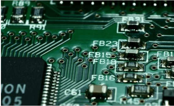
Solder Balls
· 1. The PCB silk screen holes are not aligned with the PCB pads, and the printing is not accurate, which makes the solder paste dirty the PCB.
· 2. The solder paste is exposed to too much in an oxidizing environment, and there is too much water in the air.
· 3. The heating is not precise, too slow and uneven.
· 4. The heating rate is too fast and the preheating interval is too long.
· 5. The solder paste dries too fast.
· 6. Insufficient flux activity.
· 7. Too many tin powders with small particles.
· 8. The flux volatility is inappropriate during the reflow process. The process approval standard for PCB solder balls is: when the distance between the pads or printed wires is 0.13mm, the diameter of the solder balls cannot exceed 0.13mm, or there can be no more than five solder balls within a 600mm square area.
· Bridging: Generally speaking, the cause of the solder bridge is that the solder paste is too thin, including low metal or solid content in the solder paste, low thixotropy, easy squeezing of the solder paste, and too large solder paste particles. The surface tension of the flux is too small. Too much solder paste on the pad, too high peak reflow temperature, etc.
· Open: Reason:

· 1. The amount of solder paste is not enough.
· 2. The coplanarity of component pins is not enough.
· 3. The tin is not wet enough (not enough to melt, and the fluidity is not good), and the tin paste is too thin to cause tin loss.
· 4. The pin sucks tin (like rush grass) or there is a connection hole nearby. The coplanarity of the pins is particularly important for fine-pitch and ultra-fine-pitch pin components. One solution is to apply tin on the pads in advance. The pin sucking can be prevented by slowing down the heating speed and heating the ground more and less heating on the top. It is also possible to use a flux with slow wetting speed and high activation temperature or a solder paste with different ratios of Sn/Pb to retard melting to reduce pin absorption.
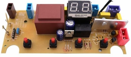
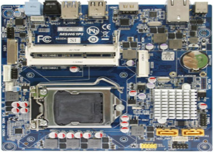
Emergency Treatment of BGA Packaged Integrated Circuit Welding
Now more and more high-density, high-performance, multi-pin large-scale PCB integrated circuits adopt ball grid array packaging, referred to as BGA. Most of these integrated circuits are high-speed processing and high-power processors, decoders, etc./heat generation. Because the pins of the BGA chip are directly below the chip, the PCB chip pins of the BGA package are connected with the solder ball and the circuit board pad, so the chip heat causes the chip pin to be unsoldered from the solder ball on the circuit board pad, Can not be repaired with a general electric soldering iron. The best way to repair is to reset the solder ball to the chip and re-solder it with a BGA soldering station, but the general repairer does not necessarily have this equipment. Blow-welding the chip with a hot air gun has certain risks, but proper use can make the chip and the circuit board re-soldered. Emergency treatment methods for the virtual soldering of BGA packaged integrated circuits under amateur conditions:
1. Soldering paste must be used, which is used to remove the surface oxides of PCB devices, reduce the surface tension of the solder, and make the solder beads and the pad better fused. The solder paste must be neutral and non-corrosive. The paste is a light yellow% colored viscous substance. Use a screwdriver to spread the paste around the chip, and then use a heat gun to heat the solder paste around the chip at a low temperature to make it drip to the chip. (When heating, you can move the circuit board in four directions. Repeatedly several times, more solder paste infiltrates the solder ball).
2. Use a hot air gun to heat the chip. It is recommended to use the medium and high temperature gear. When heating, the air duct blows and solders the chip vertically. The air duct can move clockwise or counterclockwise at a constant speed around the circumference of the chip substrate to make the middle silicon wafer of the PCB chip. All other parts are heated evenly. The control of the heating time is the key: if the time is too short, the tin balls will not melt, and the soldering will be poor; if the heating time is too long, the tin balls will burst easily, causing short circuits between the pins and damaging the chip. Therefore, observe the reaction of the soldering paste. If a small amount of blue smoke comes out, it means that the soldering paste will boil and evaporate, and the heating should be stopped immediately.
3. Use a screwdriver to press in the middle of the PCB chip and apply a certain amount of pressure. The purpose is to make the tin bead contact the chip and the PCB well, and wait for the temperature to drop, (touch the chip without hot), and then release it. After this treatment, the machine may be repaired.