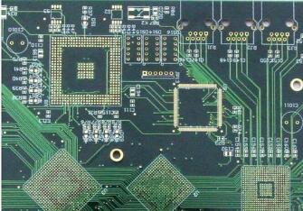
We see that there are three trends in PCB board design, the development and changes of electronic technology will inevitably bring many new problems and new challenges to PCB design. First, due to the increasing physical limits of high-density pins and pin sizes, resulting in low deployment rates; secondly, the timing and signal integrity problems caused by the increase in system clock frequency; thirdly, engineers hope to be able to use the PC platform Use better tools to complete complex and high-performance designs. Therefore, it is not difficult for us to see that PCB board design has the following three trends.

1. The design of high-speed digital circuits (that is, high clock frequency and fast edge rate) has become the mainstream.
Product miniaturization and high performance must face the problem of distribution effect caused by mixed signal design technology (ie, digital, analog and RF mixed design) on the same PCB board.
The increase in design difficulty has caused the traditional design process and design methods, and the CAD tools on the PC to be difficult to meet the current technical challenges. Therefore, the transfer of the EDA software tool platform from the UNIX to the NT platform has become a recognized trend in the industry.
2, high-frequency PCB wiring skills
High-frequency circuits tend to have high integration and high wiring density. The use of multi-layer boards is not only necessary for wiring, but also an effective means to reduce interference.
The less the lead bends between the pins of high-frequency circuit devices, the better. The lead wire of high-frequency circuit wiring is best to adopt a full straight line, which needs to be turned. It can be turned by 45° broken line or circular arc. This requirement is only used to improve the fixing strength of copper foil in low-frequency circuits, while in high-frequency circuits, it can meet this requirement. One requirement can reduce the external emission and mutual coupling of high-frequency signals.
The shorter the lead of the high-frequency circuit device pin, the better.
The fewer lead layers of high-frequency circuit device pins alternate, the better. That is, the fewer vias (Via) used in the component connection process, the better. It is measured that one via can bring about 0.5pF distributed capacitance, and reducing the number of vias can significantly increase the speed.
For high-frequency circuit wiring, pay attention to the crosstalk introduced by the signal lines in close parallel routing. If parallel distribution cannot be avoided, a large area can be arranged on the opposite side of the parallel signal lines to greatly reduce interference. It is almost unavoidable to run horizontally in the same layer, but the directions of the two adjacent layers must be perpendicular to each other.
Implement ground wire enclosing measures for particularly important signal lines or local units.
Various signal wires cannot form loops, and ground wires cannot form current loops.
3. high-frequency decoupling capacitor should be set near each integrated circuit block (IC), and the decoupling capacitor should be as close as possible to the Vcc of the device.
When the analog ground wire (AGND), digital ground wire (DGND), etc. are connected to the public ground wire, high-frequency choke should be used. In the actual assembly of the high-frequency choke link, the high-frequency ferrite bead with a wire in the center is often used. It can be used as an inductor in the schematic diagram, and a component package and wiring are defined separately for it in the PCB component library. Move it manually to a suitable position close to the common ground line.