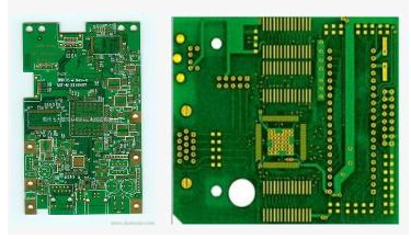
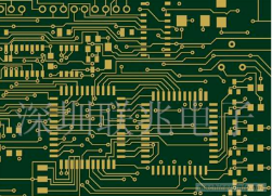
For most circuit boards, how to set the number of panels for PCBA board processing, and what factors need to be considered? How to join the board can improve the production efficiency and reduce the loss of the board. Now that there are so many benefits of splicing, after the PCB design engineer has determined the shape of the PCB, he can design the circuit board. Then PCB puzzle is a problem that needs to be dealt with in the process of PCBA processing.
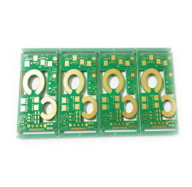
Common ways to join boards: there are many ways to join circuit boards, such as two-in-one, three-in-one, four-in-one, etc. The more common one is to combine more than two pieces of the same circuit board into a large circuit board; use different shapes Circuit boards can also be assembled, but the application is relatively small, mainly because the number of boards of different shapes is difficult to match during production; the positive and negative sides of the same kind of circuit board are combined into a circuit board, and the positive and negative boards can be Improve SMT chip processing efficiency, suitable for circuit boards with a small number of components. The Yin-Yang board design is not suitable for all circuit boards. If heavier components are designed on one side of the circuit board, the use of the Yin-Yang board may cause the heavy parts to fall when the side is used as the second part. There are also boards with large-area heat-absorbing components on the board, and the yin and yang board design cannot be used. The disadvantage of yin-yang board is that there are restrictions on SMT processing, which can easily cause uneven heating. It is necessary to consider various factors in the specific way of splicing.

The impact of board making cost on the number of jigsaw puzzles
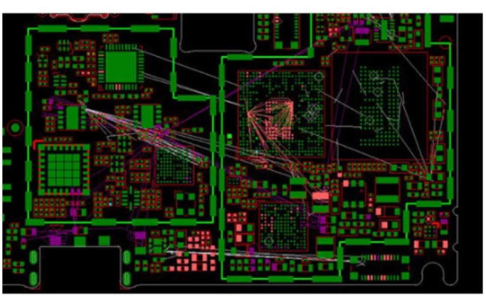
Board-making cost is the most important factor used to measure the number of jigsaw puzzles. In order to improve production efficiency and reduce costs, circuit board manufacturers will have basic standard board sizes. These standards repeatedly consider the best utilization of circuit board boards. Common standards are 16.16"x16.16", 18.32"x18.32", 20.32"x20.32",... etc. The cost of the circuit board will be affected by the size of the board used. Choosing the most suitable standard board to achieve the optimal utilization of the board can reduce the production cost of the circuit board. The cost of the circuit board is also related to factors such as the number of layers of the board, the number of holes, and whether there are blind and buried vias.
SMT processing line is divided into long line and short line according to different requirements. There are at most two fast placement machines and one slow placement machine for short-term lines; there are usually multiple fast placement machines and slow-speed placement machines for long-term lines. Usually each line is equipped with a solder paste printing machine. It takes about 35-40 seconds to brush the solder paste on the board with a length of 150mm. The two-in-one board is processed in SMT short-term, and the time allocated for each machine is about 10-26 Seconds, the placement time is much lower than the solder paste printing time, indicating that the placement machine is waiting for the solder paste printing machine, and the production capacity of the placement machine is not fully utilized. Replace the two-in-one with four-in-one, and the efficiency will be improved immediately
PCB factories usually hope that the fewer the number of panels, the better, because the smaller the number of panels, the less chance of X-boards, which can reduce the scrap rate and reduce the cost of board manufacturing. SMT factories also don't like to hit X boards, because hitting X boards will reduce the efficiency of processing. Therefore, we still have to calculate the most affordable number of panels from the perspective of overall PCBA processing costs. The process capabilities of PCB factories and SMT factories also have an impact on this. In addition, consider whether to use the V-cut or Router process to remove the edge of the board. This will also affect the panel design.
How to control the quality of PCBA processing? Let's also introduce it below!
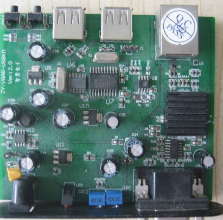
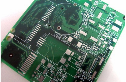
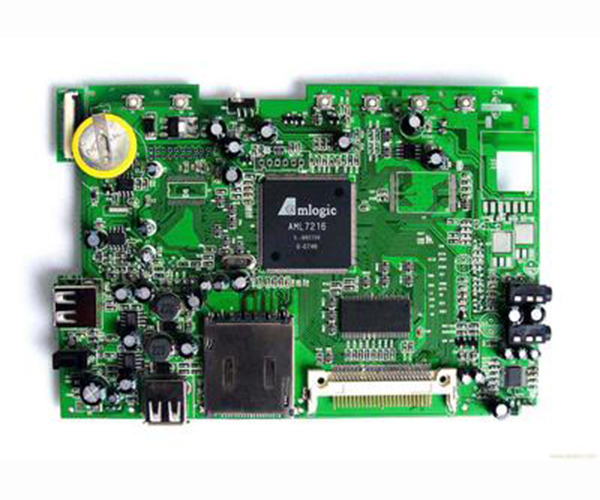
The PCBA manufacturing process involves many links. The quality of each link must be controlled to produce a good product. The general PCBA is made up of: PCB circuit board manufacturing, component procurement and inspection, SMT patch processing, plug-in processing, A series of processes such as program firing, testing, aging, etc., let us carefully explain the points that need to be paid attention to in each link. 1. After receiving the PCBA order, PCB circuit board manufacturing, analyze the Gerber file, pay attention to the relationship between the PCB hole spacing and the board's bearing capacity, do not cause bending or breakage, and whether the wiring takes into account high-frequency signal interference, impedance and other key factors . 2. Component procurement and inspection. Component procurement needs to strictly control channels, and must be picked up from large traders and original factories, and 100% avoid second-hand materials and fake materials. In addition, a special inspection post for incoming materials is set up, and the following items are strictly inspected to ensure that the components are free of faults. Reflow oven temperature test, no flying lines, whether the vias are blocked or leaking ink, whether the board surface is bent, etc.; IC checks whether the silk screen is completely consistent with the BOM, and keeps it at constant temperature and humidity;
Other common materials: check the silk screen, appearance, power-on measurement, etc. The inspection items are carried out according to the random inspection method, and the ratio is generally 1-3%. SMT Assembly processing: Solder paste printing and reflow oven temperature control are key points. It is very important to use laser stencils of good quality and meeting process requirements. According to the requirements of PCB, some steel mesh holes need to be enlarged or reduced, or U-shaped holes are used to make steel mesh according to process requirements. The furnace temperature and speed control of the reflow soldering is very critical to the solder paste infiltration and soldering reliability. It can be controlled in accordance with the normal SOP operation guidelines. In addition, AOI testing needs to be strictly implemented to minimize the defects caused by human factors. DIP plug-in processing. In the plug-in process, the mold design for wave soldering is the key point. How to use molds to maximize the probability of good products after the furnace is a process that PE engineers must continue to practice and summarize experience. In the previous DFM report, you can suggest to customers to set some test points (Test Points) on the PCB. The purpose is to test the continuity of the PCBA circuit after all the components are soldered on the PCB. If you have conditions, you can ask the customer to provide a program, and burn the program into the main control IC through a burner (such as ST-LINK, J-LINK, etc.), and you can more intuitively test the effects of various touch actions. Functional changes to verify the functional integrity of the entire PCBA. PCBA board test For orders with PCBA test requirements, the main test content includes ICT (In Circuit Test), FCT (Function Test), Burn In Test (aging test), temperature and humidity test, drop test, etc., according to customer requirements Operate the test plan and summarize the report data.