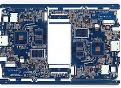
Electromagnetic compatibility (EMC) design method in PCB, the choice of PCB substrate and the setting of the number of PCB layers, the choice of electronic components and the electromagnetic characteristics of electronic components, component layout, and the length and width of the interconnection lines between components, all restrict the electromagnetic compatibility of the PCB. The integrated circuit chip (IC) on the PCB is the main energy source of electromagnetic interference (EMI). Conventional electromagnetic interference (EMI) control technology generally includes: reasonable layout of components, reasonable control of wiring, reasonable configuration of power lines, grounding, filter capacitors, shielding and other measures to suppress electromagnetic interference (EMI) are very effective, Is widely used in engineering practice.
1. Wiring rules in the electromagnetic compatibility (EMC) design of high-frequency digital circuit PCB
High-frequency digital signal cables should be short, generally smaller than 2inch (5cm), and the shorter the better.
The main signal lines are best concentrated in the center of the PCB board.
The clock generating circuit should be near the center of the PCB board, and the clock fan-out should be wired in daisy chain or parallel.
The power line should be as far away as possible from the high-frequency digital signal line or separated by the ground line. The distribution of the power supply must be low inductance (multi-channel design). The power layer in the multi-layer PCB is adjacent to the ground layer, which is equivalent to a capacitor, which plays a filtering role. The power line and ground line on the same layer should be as close as possible. The copper foil around the power layer should be retracted 20 times the distance between the two plane layers than the ground layer to ensure that the system has better EMC performance. The ground plane should not be divided. If the high-speed signal line is to be divided across the power plane, several low-impedance bridge capacitors should be placed close to the signal line.
The wires used for the input and output terminals should try to avoid being adjacent and parallel. It is best to add ground wires between wires to avoid feedback coupling.
 design")
When the thickness of the copper foil is 50um and the width is 1-1.5mm, the temperature of the wire will be less than 3 degree Celsius through a current of 2A. As far as possible, the wires of the PCB board should be as wide as possible. For integrated circuits, especially the signal wires of digital circuits, usually 4mil-12mil wire width is used. The power and ground wires are better to use a wire width greater than 40mil. The minimum spacing of the wires is mainly determined by the insulation resistance and breakdown voltage between the wires in the worst case, usually a wire spacing of more than 4mil is selected. In order to reduce the crosstalk between the wires, the distance between the wires can be increased if necessary, and the ground wire can be inserted as the isolation between the wires.
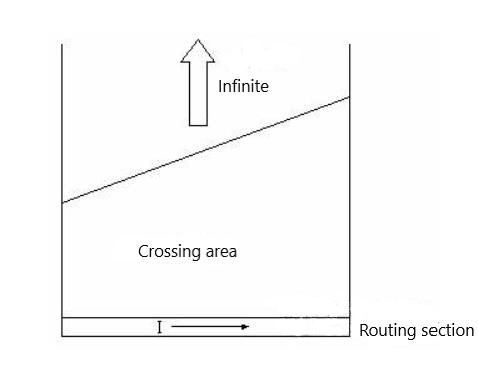
In all layers of the PCB, digital signals can only be routed in the digital part of the circuit board, and analog signals can only be routed in the analog part of the circuit board. The ground of the low-frequency circuit should be grounded in parallel at a single point as much as possible. When the actual wiring is difficult, it can be partially connected in series and then grounded in parallel. To realize the division of analog and digital power supplies, the wiring cannot cross the gap between the divided power supplies. The signal line that must cross the gap between the divided power supplies should be located on the wiring layer close to the large area ground.
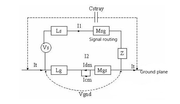
There are two main electromagnetic compatibility problems caused by power supply and ground in PCB, one is power noise, and the other is ground noise. According to the size of the PCB board current, try to enlarge the width of the power line and reduce the loop resistance. At the same time, make the direction of the power line and ground line consistent with the direction of data transmission, which helps to enhance the anti-noise ability. At present, the noise of the power supply and ground plane can only be set to the default value through the measurement of prototype products or the capacity of decoupling capacitor by experienced engineers based on their experience.
2. Layout rules in the electromagnetic compatibility (EMC) design of high-frequency digital circuit PCB
The layout of the circuit must reduce the current loop, and shorten the connection between high-frequency components as much as possible. The distance between the susceptible components should not be too close, and the input and output components should be as far away as possible.
Arrange the position of each functional circuit unit according to the circuit flow, so that the layout is convenient for signal circulation, and the signal is kept in the same direction as possible.
Take the core component of each functional circuit as the center and lay out around it. The components should be evenly, neatly and compactly arranged on the PCB, and the lead connections between the components should be shortened as much as possible.
The PCB is partitioned into independent and reasonable analog circuit areas and digital circuit areas, and the A/D converters are placed across partitions.
One of the conventional methods of PCB electromagnetic compatibility design is to configure appropriate decoupling capacitors on each key part of the PCB.