PCB signal integrity (SI) analysis, signal Integrity (Signal Integrity) is abbreviated as SI, which refers to the quality of the signal on the signal line, and is the ability of the signal to respond with the correct timing and voltage in the circuit.
The high switching speed of integrated circuit chips (IC) or logic devices, incorrect layout of termination components or incorrect wiring of high-speed signals can cause such as reflection, crosstalk, overshoot, and undershoot. Signal integrity problems such as undershoot) and ringing (ringing) may cause the system to output incorrect data, and the circuit may not work properly or even not work at all.
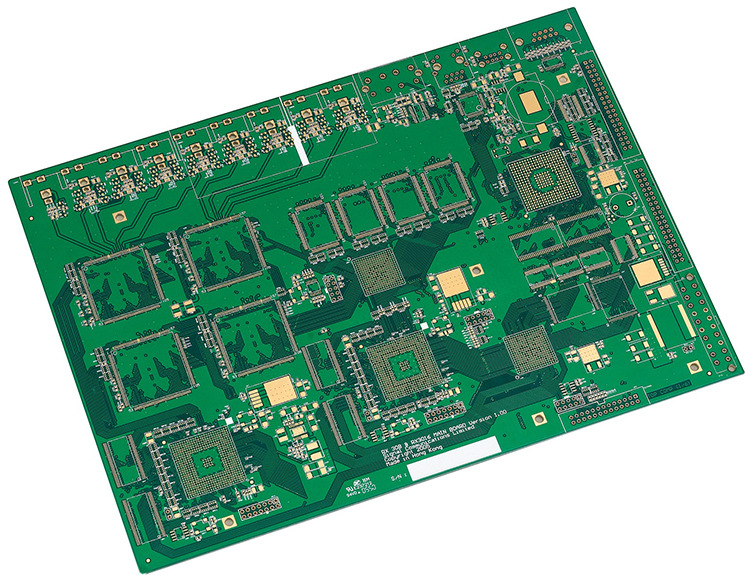
PCB signal integrity and design
In PCB design, PCB designers need to integrate the layout and wiring of components and which SI problem solving methods should be used in each case to better solve the signal integrity problem of the PCB board. In some cases, the choice of IC can determine the number and severity of SI problems. Switching time or edge rate refers to the rate of IC state transition. The faster the IC edge rate, the higher the possibility of SI problems. It is very important to correctly terminate the device.
The commonly used method to reduce signal integrity problems in PCB design is to add termination components on the transmission line. In the process of termination, it is necessary to weigh the requirements of the number of components, signal switching speed and circuit power consumption. For example, the addition of termination components means that PCB designers have less space for wiring, and it will be more difficult to add termination components in the later stages of the layout process, because appropriate space must be reserved for new components and wiring. Therefore, at the beginning of the PCB layout, it is necessary to figure out whether termination components need to be placed.

1. General guidelines for signal integrity design
How to define the number of layers of the PCB? How many layers are included? How to arrange the contents of each layer the most reasonable? For example, there should be several layers of signal layer, power layer and ground layer, and how to alternately arrange the signal layer and ground layer.
How to design a variety of power supply block systems? Such as 3.3V, 2.5V, 3V, 1.8V, 5V, 12V and so on. The reasonable division of the power layer and the common ground problem are a very important factor for the stability of the PCB.
How to configure decoupling capacitors? Using decoupling capacitors to eliminate noise is a common method, but how to determine its capacitance? Where is the capacitor placed? What type of capacitor is used?
How to eliminate ground bounce noise? How does ground bounce noise affect and interfere with useful signals?
How to eliminate the return path noise? In many cases, the unreasonable circuit design is the key to the failure of the circuit, and the circuit design is often the most helpless work for engineers.
How to design the current distribution reasonably? Especially the design of the current distribution in the electric/ground layer is very difficult, and if the total current is not evenly distributed in the PCB board, it will directly and obviously affect the unstable operation of the PCB board.
In addition, there are some common signal distortion problems such as overshoot, undershoot, ringing, transmission line delay, impedance matching, crosstalk, glitches, etc., but these problems are inseparable from the above problems, and there is a causal relationship between them.
2. PCB design guidelines to ensure signal integrity
The earlier the signal integrity (SI) problem is solved, the higher the efficiency of the design, which can avoid adding termination components after the circuit board design is completed.
With the increase of IC output switching speed, almost all designs have encountered signal integrity problems regardless of the signal period. Even if there is no SI problem in the past, as the operating frequency of the circuit increases, the signal integrity problem will definitely be encountered.
SI and EMC experts need to perform simulation and calculations before PCB routing. Then, PCB board design can follow a series of very strict design rules. Where there are doubts, you can add termination components to obtain as much SI as possible. Safety margin.
Power integrity (PI) and signal integrity (SI) are closely related, and power integrity directly affects the signal integrity of the final PCB board. And in many cases, the main cause of signal distortion is the power supply system.