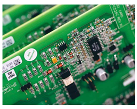
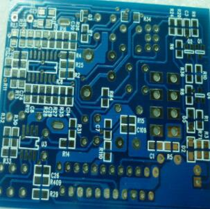
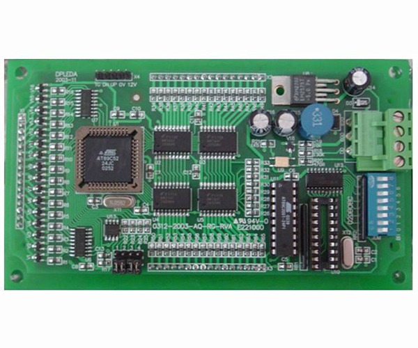
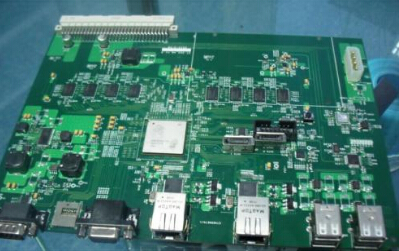
PCB soldering is an important process in the assembly process of electronic products. The quality of welding directly affects the performance of electronic circuits and electronic devices.
Excellent soldering quality can provide good stability and reliability for the circuit. Poor soldering methods can cause damage to the components, bring great difficulties to the test, and sometimes leave hidden dangers that affect the reliability of electronic equipment.
1. Classification and characteristics of PCB patch welding
Welding is generally divided into three categories: fusion welding, contact welding and brazing.
Fusion welding: refers to the method of heating the weldment joint to a molten state during the welding process and completing the welding without applying pressure. Such as arc welding, gas welding, etc.
Contact welding: During the welding process, pressure (heated or not) must be applied to the weldment to complete the welding. Such as ultrasonic welding, pulse welding, friction welding, etc.
Soldering: The so-called "soldering" in the installation process of electronic products is a kind of soft soldering, mainly using low melting point alloy materials such as tin and lead as solder, so it is commonly called "soldering".
Second, the principle of PCB patch welding
The soldering of electronic circuits seems simple. It seems to be just a process of combining molten solder and the metal to be welded (base metal), but its microscopic mechanism is very complicated, which involves physics, chemistry, materials science, electricity, etc. knowledge. Familiar with the basic theory of welding, can we know the various problems in welding and deal with it freely, so as to improve the welding quality of solder joints.

The so-called welding is a process in which the solder and the metal to be welded are heated to the optimal temperature at the same time, and the molten solder fills the gap between the metal and forms a metal alloy combination with it. From a microscopic point of view, welding includes two processes: one is the wetting process, and the other is the diffusion process.
1. Wetting (lateral flow)
Also known as wetting, it means that the molten solder forms a uniform, smooth, continuous and firmly adhered solder layer on the metal surface.
The degree of wetting is mainly determined by the cleanliness of the surface of the weldment and the surface tension of the solder.
The metal surface looks relatively smooth, but under the microscope, there are countless unevenness, grain boundaries, and scars. The solder is wetted and diffused by capillary action along the bumps and scars on these surfaces, so soldering It should make the solder flow.
The flow process is generally that the rosin removes the oxide film in the front, and the solder follows it, so the wetting is basically the molten solder flowing laterally along the surface of the object.
2. Diffusion (vertical flow)
Along with the wetting phenomenon in which molten solder spreads on the surface to be soldered, the solder spreads into the solid metal. For example, when soldering copper parts with tin-lead solder, there are surface diffusion, grain boundary diffusion and intragranular diffusion during the soldering process. The lead in tin-lead solder only participates in surface diffusion, while tin and mace atoms diffuse each other, which is the selective diffusion determined by the properties of different metals. It is precisely because of this diffusion that a new alloy is formed at the interface between the two, so that the solder and the weldment are firmly combined.
3. Metallurgical bonding
As a result of the diffusion, an alloy layer is formed at the junction of the tin atoms and the copper metal to be welded, thereby forming a strong solder joint. Take tin-lead solder soldering copper parts as an example. Under low temperature (250~300 degree Celsius) conditions, Cu3Sn and Cu6Sn5 will be formed at the interface of copper and solder. If the temperature exceeds 300 degree Celsius, in addition to these alloys, intermetallic compounds such as Cu31Sn8 will also be formed. The thickness of the solder joint interface varies with temperature and soldering time, generally between 3~10um.
Three, the elements of PCB patch welding
1. The weldability of welding base metal
The so-called solderability means that the liquid solder and the base metal should be able to dissolve each other, that is, there must be a good affinity between the two types of atoms. The degree of mutual melting of two different metals depends on the atomic radius, their position in the periodic table and the crystal type. Tin-lead solder, in addition to metal materials containing a large amount of chromium and aluminum alloys that are not easily soluble in each other, most of them are mutually soluble with other metal materials. In order to improve the solderability, measures such as tin plating and silver plating on the surface are generally adopted.
2. Cleanliness of welding parts
The surface of the solder and the base metal must be "clean", where "clean" means that there is no oxide layer between the solder and the base metal, let alone pollution. When there is oxide or dirt between the solder and the metal to be welded, it will hinder the free diffusion of molten metal atoms and will not produce wetting effect. Oxidation of component pins or PCB pads is one of the main reasons for "virtual soldering".
3. Flux
The flux can destroy the oxide film, purify the soldering surface, and make the solder joints smooth and bright. The flux in electronic assembly is usually rosin.
4. Soldering temperature and time
The best soldering temperature is 250±5oC, and the lowest soldering temperature is 240oC. The temperature is too low to easily form cold solder joints. Above 260oC, the quality of solder joints will deteriorate.
Welding time: It takes 2~3S to complete the two processes of wetting and diffusion, and 1S only completes 35% of the two processes of wetting and diffusion. Generally, the welding time of IC and triode is less than 3S, and the welding time of other components is 4~5S.
5. Welding method
The welding method and procedure are very critical.
Fourth, the quality standard of PCB patch solder joints
1. Good electrical performance
High-quality solder joints should make the solder and the surface of the metal workpiece form a solid alloy layer to ensure good electrical conductivity. Simply stacking the solder on the surface of the metal workpiece to form a virtual weld is a taboo in welding.
2. Has a certain mechanical strength
Electronic equipment sometimes needs to work in a vibrating environment. In order to prevent the weldment from loosening or falling off, the solder joint must have a certain mechanical strength. The strength of tin and lead in tin-lead solder is relatively low. In order to increase the strength, the soldering surface can be increased as needed. Or the component leads and wires are meshed, twisted, and hooked to the contacts before welding.
3. The amount of solder on the solder joints should be appropriate
Too little solder on the solder joints will not only reduce the mechanical strength, but also cause early failure of the solder joints; too much solder on the solder joints will increase the cost and easily cause solder joint bridging (short circuit), and will also conceal soldering defects. So the amount of solder on the solder joints should be appropriate. When soldering a printed circuit board, it is most suitable when the solder fills the pads and spreads out in a skirt shape.
4. The surface of the solder joints should be bright and uniform
The surface of a good solder joint should be bright and uniform in color. This is mainly because the thin film formed by the resin component that is not completely volatilized in the flux covers the surface of the solder joints, which can prevent the surface of the solder joints from oxidizing.
5. The solder joints should not have burrs and voids
There are burrs and gaps on the surface of the solder joints, which are not only unsightly, but also bring harm to electronic products, especially in the high-voltage circuit part, which will cause sharp discharge and damage electronic equipment.
6. PCB solder joint surface must be clean
If the dirt on the surface of the solder joints is not removed in time, acidic substances will corrode component leads, contacts and PCB printed circuits, and moisture absorption will cause leakage or even short-circuit burning, which will cause serious hidden dangers.