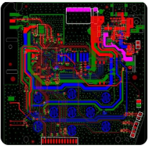
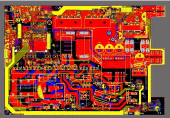
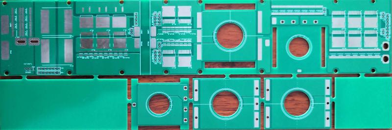
How to design the characteristic impedance
In high-speed PCB design, we often perform characteristic impedance control on high-speed signal lines to optimize signal quality. What is the characteristic impedance?
1. Transmission line principle
Before introducing the characteristic impedance, let's review the basic principles of transmission lines introduced in the "Signal Integrity Video". As shown in the figure on the left, the low-frequency circuit uses the RLGC model with lumped parameters, and the high-frequency circuit on the right uses the RLGC model with distributed parameters.
Solving the transmission line calculus equation is easy for you, and I won’t introduce it here. The result of the equation is that we can get the attenuation constant, characteristic impedance, phase shift constant, etc. of the PCB transmission line. The specific meaning is described in detail in "Signal Integrity Video". Here we mainly introduce the application of PCB characteristic impedance. The following is the formula for the characteristic impedance obtained by solving the equation, but it is not very useful because you cannot know the R, L, G, and C corresponding to the unit length.
2. The influence of characteristic impedance mismatch
The characteristic impedance of the transmission line refers to the impedance corresponding to each point on the line when high-speed signals are transmitted on the PCB line. We hope that the characteristic impedance of the transmission line will not change suddenly, because a sudden change in the transmission line will cause signal reflection, which will affect the signal quality.
3. Selection of characteristic impedance
The characteristic impedance of the PCB is determined by the matching resistance ZL at the load end, depending on the specifications of various interfaces. The characteristic impedance error is mainly affected by the PCB factory process and can generally be controlled within 5%-10%. The following is a common interface PCB impedance control.
USB differential cable 90Ω
PCIE differential line 100Ω
RF single-ended transmission line 50Ω
Ordinary single-ended transmission line 50Ω

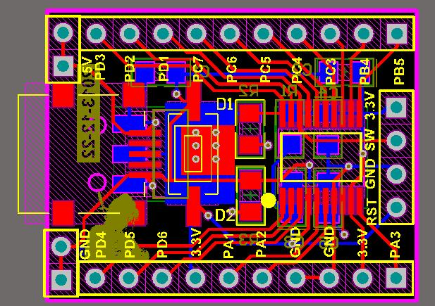
4. PCB characteristic impedance design
At present, PCB manufacturers often use polar si9000 software to calculate characteristic impedance. Let's take a single-ended signal line as an example. There are four setting parameters: dielectric constant, dielectric thickness, line width and copper foil thickness.
Dielectric constant Er1: The dielectric constant of the sheet, generally 4.2-4.5 for FR4 sheet.
Medium thickness H1: the thickness of the sheet or PP.
Line width W1/W2: the line width of PCB wiring.
Copper foil thickness: According to the actual situation, there are 0.5/1/2 OZ and so on.
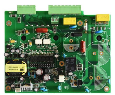
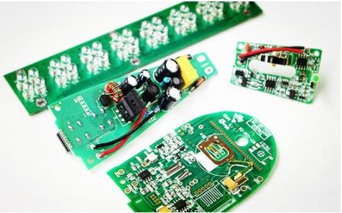
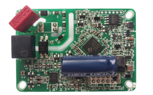
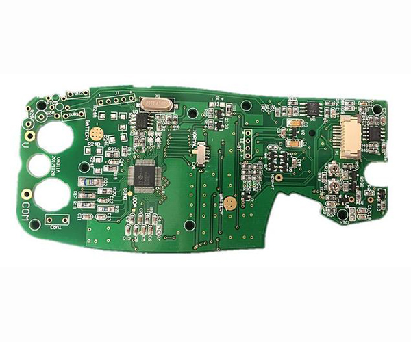
Wireless charging scheme launches PCBA
5W/7.5W/10W/15W power adaptive; built-in 32bit high-performance processor; support QI (BPP\EPP) certification, in line with WPC1.2.4 protocol; high-precision FOD algorithm; integrated Dual-Channel fully synchronous digital demodulation; support OCP/OVP/OTP; support QC2.0/QC3.0/AFC; support DPL dynamic power adjustment; support simultaneous charging of multiple devices; support function customization; support USB upgrade.
The product features are as follows:
1. Single chip 5W/10W transmitter solution
2. Suitable for Type A6/A11/A28/MP-A2 etc.
3. Passed WPC 1.2.4 certification
4. Support 10W fast charge protocol
5. The efficiency is as high as 85% fast charge, 78%
6. Integrated synchronous dual-channel all-digital demodulation circuit
7. Over temperature, over voltage, software/hardware double over current and short circuit protection
8. FOD function
9. Dynamic power lock
10. Enhanced vertex shutdown
11. Adaptive input voltage 5V/9V
12. Support multiple transmitters to share input power
Products have been widely used in:
l Smart phones and smart wearables
l Automotive electronics
l Medical
l Furniture, digital products
l Power bank
l Home office, airport and restaurant chain wireless charging platform and many other fields
Cooperation model
◆Customized development of wireless charging technology solutions for various electronic products
◆Production of wireless charger products and finished products
◆ Sell wireless charging PCBA
◆Sell the core MCU of wireless charging authorization
◆Other parties negotiate and cooperate mode
Our advantage: ☑ complete goods
☑ Professional service
☑ Original authentic
☑ Efficient procurement
☑ Save time and effort