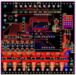
Effectively control the whole process of hardware development of PCB board design and development to ensure that the developed PCB controller hardware can meet customer requirements and corresponding national standards.
Scope
It is suitable for the development of new controller products and the improvement of finalized products.
Duties
In the case of control board design and development needs, a development team is established. The team members are composed of product development supervisors, hardware engineers, test engineers and reliability engineers.
The product development supervisor is responsible for preparing and supervising the implementation of the project development plan, as well as the organization, coordination and management of the design and development process, as well as the organization of design review, design verification, and design confirmation.
The hardware engineer is responsible for the selection, design, PCB board design and debugging of the hardware circuit. The test engineer is responsible for the testing of hardware circuit prototypes and finished products.

The reliability engineer is responsible for the reliability design and verification of the hardware circuit.
Establishment of the development team
The PCB product development supervisor sets up a hardware development team according to the development tasks and compiles the "Hardware Product Development Plan", which will be implemented after approval by the superior. The "Hardware Product Development Plan" includes the following: Design and development phases.
Suitable for all stages of PCB design review, verification and confirmation activities and the materials required for these activities.
Tasks, responsible persons, and schedule requirements for each stage.
The "Development Plan" should be updated in time with the adjustment of the design and development progress, and be implemented after being approved by the project team and reported to the superior.
There are five methods for choosing control board welding, each with different advantages:
Solution 1. Manual welding Manual welding is suitable for product trial production, small batch production of electronic products, debugging and maintenance of electronic products, and some occasions that are not suitable for automatic welding.
This method requires simple welding tools, simple welding steps, and easy to master, and is mainly suitable for situations where there are not many electronic component pins.
Solution 2: The characteristics of PCB dip soldering: simple operation, no missing soldering, high production efficiency; but it is easy to cause defects such as false soldering, and soldering is required to correct the solder joints; improper control of the solder bath temperature will cause the printed board Warping, deformation, damage to components.
This solution requires high PCB soldering tools, which is not economical for students to learn.
Solution three, wave soldering The characteristics of wave soldering: high production efficiency, most suitable for large-volume soldering of single-sided printed circuit boards; soldering temperature, time, solder and flux, etc., can be more fully controlled.
However, wave soldering is prone to cause the phenomenon of solder joint bridging, which requires repair soldering. This program has higher requirements for welding tools and is not economical for students to learn.
Solution four, reflow soldering (reflow soldering) This technology is mainly used for soldering of SMD components. The components to be welded receive little thermal shock and will not be damaged due to overheating; there are no bridge defects, and the quality of the solder joints is high.
This solution requires high PCB soldering tools, which is not economical for students to learn, and soldering technology cannot be mastered quickly.
Scheme 5: PCB contact welding (Wuxi welding) This scheme is more practical for occasions such as connecting cables to PCB terminals. It has no practical value for PCB welding of radios, and it is not economical for students.