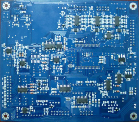
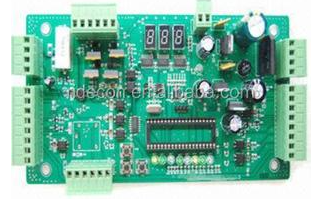
In PCB design, engineers will inevitably face many problems, the following summarizes the ten common problems in PCB design, hoping to play a certain role in avoiding everyone in PCB design.
One, the character is misplaced
1. character cover pad SMD weld, to the printed circuit board on/off test and component welding inconvenience.
2. the character design is too small, resulting in screen printing difficulties, too large to make the characters overlap each other, it is difficult to distinguish.
Second, graphic layer abuse
1. Some useless lines were made on some graphic layers. Originally, more than five lines were designed for four layers, which caused misunderstanding.
2. Save trouble in design. Protel software is used as an example to draw lines with Board layer and mark lines with Board layer.
3. violation of conventional design, such as component surface design in the Bottom layer, welding surface design in the Top, causing inconvenience.
Three, the overlap of pads
1. The overlap of the pad (in addition to the surface of the pad) means the overlap of the hole. In the drilling process, the drill bit will be broken because of multiple drilling in one place, leading to the damage of the hole.
2. The two holes in the multi-layer plate overlap, such as a hole for the isolation plate, the other hole for the connection plate (weld), so draw the film after the performance of the isolation plate, resulting in scrap.
Four, single-sided pad aperture setting
1. Single-sided pads generally do not drill, if the drilling needs to be marked, the aperture should be designed for zero. If the values are designed so that the hole coordinates appear at this location when the borehole data is generated, the problem arises.
2. Single side pads such as drilling should be specially marked.
Fifth, the electric formation is also the flower pad and the connection
Because the power supply is designed as a flowered pad, the stratum is the opposite of the image on the actual printed board, and all the lines are isolated lines, which should be very clear to the designer. Here, by the way, care should be taken when drawing isolation lines for groups of power sources or fields, so as not to leave gaps that would short-circuit the two groups of power sources or cause an area blockade of the connection (so that a group of power sources is separated).
Six, draw the pad with the filling block
Drawing pads with filler blocks can pass DRC inspection when designing the circuit, but not for processing. Therefore, the solder block can not directly generate solder blocking data. When applying solder blocking agent, the filling block area will be covered by solder blocking agent, resulting in welding difficulty of the device.
Seven, processing level definition is not clear
1. Single panel design in the top layer, if you do not add instructions on the positive and negative, may be produced by the board installed on the device and not good welding.
2. For example, a four-layer board is designed with TOP MID1, MID2 BOTTOM four layers, but is not machined in this order, which requires explanation.

8. Too many filling blocks in the design or filling blocks with extremely thin lines
1. the phenomenon of light drawing data loss, light drawing data is not complete.
2. Because filling blocks are drawn one by one in light drawing data processing, the amount of light drawing data generated is quite large, which increases the difficulty of data processing.
Nine, the surface mount device pad is too short
This is for the on-off test, for too dense surface mount device, the spacing between the feet is quite small, the pad is also quite fine, the test needle installation, must be up and down (left and right) staggered position, such as pad design is too short, although does not affect the device installation, but will make the test needle is not wrong.
Ten. The spacing of large area grid is too small
The edge between the grid lines that constitute a large area is too small (less than 0.3mm). In the process of printed board manufacturing, a lot of broken film is likely to be attached to the board after the mapping process, resulting in wire breakage.