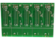
In precautions for PCB board design, for engineers, circuit design is the most basic. However, many engineers tend to be careful when designing complex and difficult PCB boards, but ignore some points to be noted when designing basic PCB boards, which leads to errors. It may cause problems or be completely broken when the perfect circuit diagram is converted into a PCB board. Therefore, in order to help engineers reduce design changes in PCB board design and improve work efficiency, here are several aspects that should be paid attention to in the PCB board design process.
1. Design of heat dissipation system in PCB board design
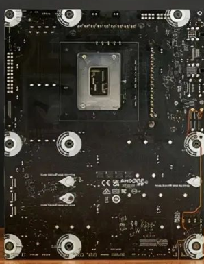
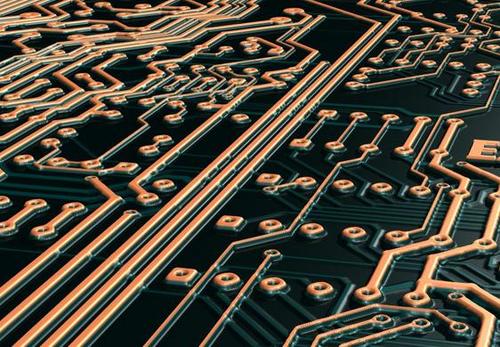
In the PCB board design, the design of the heat dissipation system includes the cooling method and the selection of heat dissipation components, as well as the consideration of the cold expansion coefficient. Nowadays, the commonly used methods of PCB board heat dissipation are: heat dissipation through the PCB board itself, and adding a heat sink and a heat conduction board to the PCB board.
In the traditional PCB board design, because the boards mostly use copper clad/epoxy glass cloth substrates or phenolic resin glass cloth substrates, and a small amount of paper-based copper clad boards are used, these materials have good electrical and processing properties, but heat conduction The performance is very poor. Because surface mount components such as QFP and BGA are used in large quantities in the current PCB board design, the heat generated by the components is transferred to the PCB board in a large amount. Therefore, the most effective way to solve the problem of heat dissipation is to improve the heat dissipation of the PCB board directly in contact with the heating element. Ability, transmitted or emitted through the PCB board.
When there are a few components on the PCB that generate a large amount of heat, a heat sink or a heat pipe can be added to the heating components of the PCB; when the temperature cannot be lowered, a heat sink with a fan can be used. When the amount of heat-generating components on the PCB is large, a large heat dissipation cover can be used, and the heat dissipation cover is buckled on the surface of the components as a whole, so that it contacts each component on the PCB to dissipate heat. For professional computers used for video and animation production, even water cooling is required to cool down.
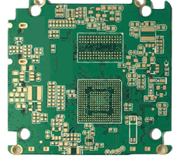
2. Selection and layout of components in PCB board design
When designing a PCB board, it is undoubtedly faced with the choice of components. The specifications of each component are different, and the characteristics of components produced by different manufacturers of the same product may be different. Therefore, for the selection of components during PCB board design, you must contact the supplier to know the characteristics of the components, and Understand the impact of these characteristics on PCB board design.
At present, choosing the right memory is also a very important point for PCB board design. Due to the continuous updating of DRAM and Flash memory, it is a big challenge for PCB board designers to make new designs not affected by the memory market. Therefore, PCB board designers must focus on the memory market and maintain close contact with manufacturers.

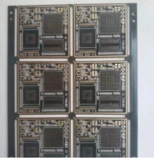
In addition, necessary calculations must be made for some components with large heat dissipation, and their layout needs special consideration. A large number of components can generate more heat when they are together, which will cause deformation and separation of the solder mask, and even ignite the entire PCB board. Therefore, the design and layout engineers of the PCB board must work together to ensure that the components have a suitable layout.
The size of the PCB board must first be considered during layout. When the PCB board size is too large, the printed lines are long, the impedance increases, the anti-noise ability is reduced, and the cost also increases; the PCB board is too small, the heat dissipation is not good, and the adjacent lines are easily interfered. After determining the size of the PCB board, determine the location of the special components. Finally, according to the functional units of the circuit, all the components of the circuit are laid out.
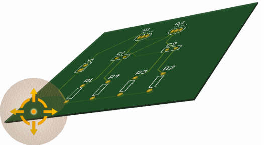
3. Testability design in PCB board design
The key technologies of PCB testability include: testability measurement, testability mechanism design and optimization, and test information processing and fault diagnosis. The testability design of the PCB board is actually to introduce a certain testability method that can facilitate the test into the PCB board, and provide an information channel for obtaining the internal test information of the tested object. Therefore, a reasonable and effective design of the testability mechanism is the guarantee for successfully improving the testability level of PCB boards. To improve product quality and reliability, and reduce product life cycle costs, testability design technology is required to quickly and easily obtain feedback information during PCB board testing, and can easily make fault diagnosis based on the feedback information. In the PCB board design, it is necessary to ensure that the detection position and the entry path of the DFT and other probes will not be affected.
With the miniaturization of electronic products, the pitch of components becomes smaller and smaller, and the mounting density will also become larger. There are fewer and fewer circuit nodes available for testing, so the online test of printed board assemblies is becoming more and more difficult. Therefore, the electrical conditions and physical and mechanical testability of the printed board should be fully considered when the PCB board is designed. Conditions, use appropriate mechanical and electronic equipment for testing.
4. Moisture sensitivity level MSL in PCB board design
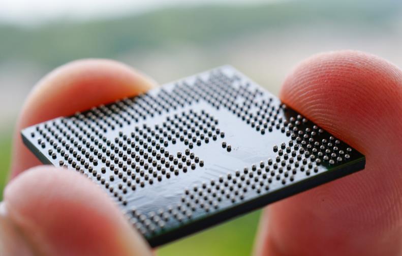
MSL: Moisure Sensitive Level, that is, the humidity sensitivity level, which is stated on the label outside the moisture-proof packaging bag. It is divided into eight levels: 1, 2, 2a, 3, 4, 5, 5a, and 6. Components with special requirements for humidity or humidity-sensitive component marks on the package must be effectively managed to provide the temperature and humidity control range of the material storage and manufacturing environment, so as to ensure the reliability of the performance of temperature and humidity sensitive components. When baking, BGA, QFP, MEM, BIOS, etc. require perfect vacuum packaging. High temperature resistant and non-high temperature resistant components are baked at different temperatures. Pay attention to the baking time. For PCB baking requirements, first refer to PCB packaging requirements or customer requirements. The humidity-sensitive components and PCB boards after baking should not exceed 12H at room temperature. Unused or unused humidity-sensitive components or PCB boards that do not exceed 12H at room temperature must be sealed in a vacuum package or placed in a dry box. put.
The above four points to pay attention to when designing PCB boards are hoped to be helpful to engineers struggling in PCB board design.