Increase the distance between the lines to make the mutual inductance between the interference source and the induced line as small as possible
PCB layout and layout
If possible, make the line of the interference source and the induced line be at right angles (or close to right angles) wiring, which can greatly reduce the coupling between the two lines
PCB layout and layout
Increasing the distance between lines is the best way to reduce capacitive coupling
PCB layout and layout
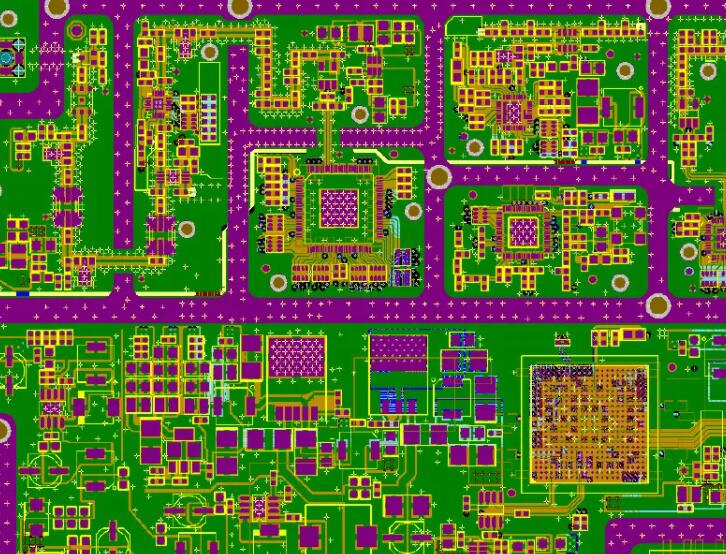
Before the formal wiring, the first thing is to classify the wiring. The main classification method is based on power level, divided into several groups at every 30dB power level
PCB layout and layout
Different types of wires should be bundled separately and laid separately. Adjacent wires can also be grouped together after taking shielding or twisting measures. The minimum distance between the classified wiring harnesses is 50~75mm

PCB layout and layout
In the resistor layout, the gain control resistors and bias resistors (up and down) of the amplifier, pull-up and pull-down and regulated rectifier circuits should be as close as possible to the amplifier, active devices and their power supply and ground to reduce their decoupling effects (improve transient response) time).
PCB layout and layout
Place the bypass capacitor close to the power input
PCB layout and layout
The decoupling capacitor is placed at the power input. As close to each IC as possible
PCB layout and layout
Basic PCB characteristics Impedance: Determined by the quality of copper and cross-sectional area. Specifically: 1 ounce 0.49 milliohms/unit area
Capacitance: C=EoErA/h, Eo: permittivity of free space, Er: permittivity of PCB substrate, A: reach of current, h: spacing between traces
Inductance: evenly distributed in the wiring, about 1nH/m
In terms of ounce copper wire, under the rolling of 0.25mm (10mil) thick FR4, located above the ground layer) 0.5mm wide, 20mm long wire can produce 9.8 milliohm impedance, 20nH inductance and ground Coupling capacitance of 1.66pF.
PCB layout and layout
Basic principles of PCB layout: increase the trace spacing to reduce crosstalk of capacitive coupling; lay power lines and ground lines in parallel to optimize PCB capacitance; lay sensitive high-frequency lines away from high-noise power lines; widen the power supply Wire and ground wire to reduce the impedance of power wire and ground wire;
PCB layout and layout
Segmentation: Use physical segmentation to reduce the coupling between different types of signal lines, especially power and ground lines
PCB layout and layout
Local decoupling: Decoupling the local power supply and the IC. Use a large-capacity bypass capacitor between the power input port and the PCB to filter low-frequency pulsation and meet the burst power requirements. Use decoupling between the power supply of each IC and the ground. Coupling capacitors, these decoupling capacitors should be as close as possible to the pin.
PCB layout and layout
Wiring separation: Minimize crosstalk and noise coupling between adjacent lines in the same layer of the PCB. The 3W specification is used to process critical signal paths.
PCB layout and layout
Protection and shunt line: adopt two-sided grounding protection measures for key signals, and ensure that both ends of the protection line must be grounded
PCB layout and layout
Single-layer PCB: The ground wire should be at least 1.5mm wide, and the jumper and ground wire width changes should be kept to a minimum
PCB layout and layout
Double-layer PCB: Use ground grid/dot matrix wiring first, keep the width above 1.5mm. Or put the ground on one side and the signal power on the other side
PCB layout and layout
Protective ring: Use the ground wire to form a ring to enclose the protective logic for isolation
PCB layout and layout
PCB capacitance: PCB capacitance is generated on the multilayer board due to the thin insulating layer between the power supply surface and the ground. The advantage is that it has a very high frequency response and a low series inductance evenly distributed over the entire surface or the entire line. It is equivalent to a decoupling capacitor evenly distributed on the entire board.
PCB layout and layout
High-speed circuits and low-speed circuits: High-speed circuits should be close to the ground plane, and low-speed circuits should be close to the power plane.
Ground copper filling: The copper filling must ensure grounding.
PCB layout and layout
The routing directions of adjacent layers are orthogonal to avoid different signal lines in the same direction on adjacent layers to reduce unnecessary inter-layer interference; when it is difficult to avoid due to board structure limitations (such as certain backplanes) In this case, especially when the signal rate is high, consider using a ground plane to isolate each wiring layer, and use a ground signal line to isolate each signal line;