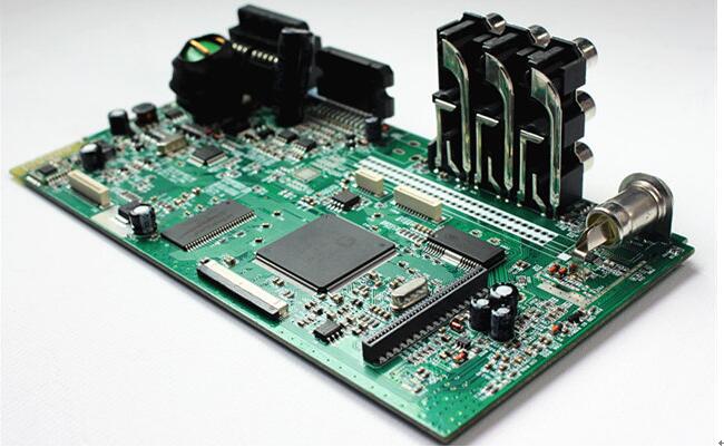
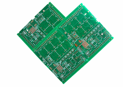
Generally speaking, PCB components carrying various electronic components must undergo a soldering process during the electronic assembly process. Wave soldering is a well-known and common soldering method. When PCB components switch to lead-free wave soldering, they will encounter many challenges. Just like any novel manufacturing technology entering product manufacturing, people may have made a pre-estimation of many related challenges and made preparations in advance.
However, there are some challenges that cannot be known in advance, and the related problems will not be exposed until after the mass production of the product, and sufficient data can be provided to provide a basis for solving these problems. Therefore, engineers often learn continuously and learn lessons and experience during the implementation of the production process.
In fact, the lead-free assembly process is not a very novel process technology.

Lead-free wave soldering has been used in practice for many years. For a long time before the RoHS regulations were enacted, electronic assembly engineers have encountered the need for higher soldering operating temperatures due to the higher melting temperature of the silver-tin electrode used.
These electronic components are designed to meet the requirements of harsh environments, and because they are relatively uncomplicated, the output is acceptable. When the RoHS regulations are introduced into the mainstream field of electronic assembly, it is relatively simple as a transitional early product, which includes consumer electronic products.
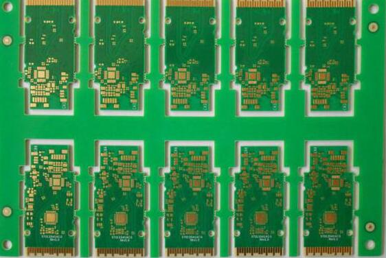
By using single-sided or double-sided PCB components, people use relatively less troublesome SMT devices on the PCB soldering surface. The lead-free transition of this type of electronic components is basically smooth sailing, and there is no need to make major changes to the process parameter settings originally derived from tin-lead alloys. In many cases, even the most primitive solders suitable for tin-lead alloys can be successfully used in lead-free process operations.
Through years of research, generally speaking, when using lead-free soldering, 1.6mm thick PCB will encounter a slightly tighter process port. The change in the requirements for preheating is not too great, and most of the current welding equipment can fully adapt to it. The soldering temperature may increase, depending on the melting temperature used in the previous tin-lead alloy process operations. Completely filling the holes with lead-free solder may encounter great challenges, especially for products that use OSP surface coating. The pause time in wave soldering may be one second or more than two seconds. In terms of draining water or reducing bridging, lead-free alloys are not as easy to handle as tin-lead alloys, so they may present problems for devices with fine pitch.
All of this, for less complex components, most of the challenges can be solved by formulating the correct parameters and using basic process control measurement techniques.
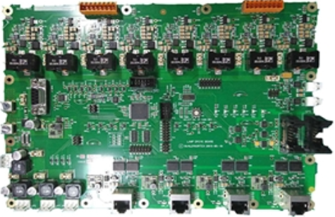
With thicker PCB circuit boards with more layers and more complex electronic components (such as the circuit boards of program-controlled switches) entering the transition period from tin-lead alloy to lead-free soldering, tin-lead alloy and lead-free The difference in process operation between chemical alloys has increased.