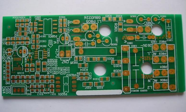
PCB factory basic technical requirements for copper plating
1. Must have good mechanical properties
The mechanical properties of the electroplated layer in the PCB factory mainly refer to toughness, which is a concept of metallurgy. In metallurgy, it is determined by relative elongation and tensile strength. The toughness Tou specified by metal science, Tou=ε*6, where ε-relative elongation, 6-tensile strength. The relative elongation ε=L-L0/L0*100%, which represents the physical quantity of the metal's deformability, and the tensile strength is the tensile force borne on a unit cross-section, which is the physical quantity of the resistance to deformation, and the toughness is a combination of the above two The index of physical quantity indicates the total energy required for the material to be broken. Generally, the relative elongation is not less than 10%, and the tensile strength is 20-50kg/m㎡, so as to ensure that after the PCB is leveled by hot air or electrical assembly, the wave soldering will not be caused by the epoxy base material and the copper plating. The difference in layer expansion coefficient causes Z-direction fracture of the copper-plated layer.
2. The ratio of the thickness of the copper plating layer on the board surface (Ts) to the thickness of the copper plating layer on the hole wall (Th) is close to 1:1
Through practical application, only the plate surface and the thickness of the plating layer in the hole can be guaranteed to have sufficient strength and conductivity. This requires that the plating solution used has a good dispersion ability. Otherwise, to make the thickness of the hole wall plating layer meet the national standard, the plating time must be prolonged. As a result, it will not only waste time and raw materials but also directly affect the subsequent imaging accuracy.
3. The plating layer is firmly bonded to the substrate. If it is not strong, the plating layer will blister and peel to a certain extent, and even the PCB will be scrapped in severe cases.
4. The plating layer should have good conductivity because the circuit board mainly relies on the electroplated copper layer to conduct electricity. To have good conductivity, the purity of the plating layer should be high, and the inclusion of impurities should be less. The impurities mainly come from the additives in the plating solution. Certain components and impurities in the anode.

5. The copper plating layer should be uniform, meticulous, and have a good appearance.
The design of PCB A/D partition and ground division
When connecting the analog ground and digital ground pins of the A/D converter together, most A/D converter manufacturers recommend connecting the analog ground and digital ground pins to the same low-impedance through the shortest lead. On the ground, because most A/D converter chips do not connect the analog ground and digital ground together, the analog ground and digital ground must be connected through external pins. Any external impedance connected to the digital ground will pass through the parasitic capacitance. More digital noise is coupled to the analog circuits inside the IC. According to this recommendation, both the analog ground (AGND) and digital ground (DGND) pins of the A/D converter need to be connected to the analog ground.
If the system has only one A/D converter, the above problems can be easily solved. Separate the ground, and connect the analog ground and digital ground together under the A/D converter.
If there are too many A7D converters in the system, if the analog ground and digital ground are connected together under each A7D converter, a multi-point connection will be generated, and the isolation between analog ground and digital ground will be meaningless., But if you don’t connect in this way, it violates the manufacturer’s requirements. Therefore, the best way is to use the unified land at the beginning and divide the unified land into an analog part and a digital part. This layout and routing not only meet the requirements of IC device manufacturers for low-impedance connection of analog ground and digital ground pins but also do not form a loop antenna or dipole antenna.
Separate ground design Some people suggest separating the digital ground and analog ground on the mixed-signal circuit board so that the isolation between the digital ground and the analog ground can be achieved. Although this method is feasible, there are also many potential problems, especially in complex large-scale systems. The most critical problem is that it cannot be routed across the division gap. Once the division gap is routed, electromagnetic radiation and signal crosstalk will increase sharply. The most common problem in PCB design is that the signal line crosses the divided ground or power supply and generates EMI problems. Mixed-signal PCB design is a complicated process, and the following points should be noted:
1) Divide the PCB into independent analog and digital parts.
2) The A/D converter is placed in partitions.
3) Do not divide the ground. Lay a uniform ground under the analog part and the digital part of the circuit board.
4) In all layers of the PCB circuit board, digital signals can only be routed in the digital part of the circuit board.
5) In all layers of the PCB circuit board, the analog signal can only be routed in the analog part of the circuit board.
6) Realize the division of analog and digital power supply.
7) The wiring cannot cross the gap between the divided power planes.
8) The signal line that must span the gap between the divided power supplies should be located on the wiring layer close to the large area ground.
9) Analyze the path and method that the return ground current actually flows through.
10) Use correct wiring rules.