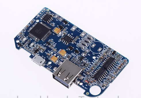
The printed circuit board (PCB) is the body of electronic products, and the performance, life and reliability of the final product depend on the electrical system it constitutes. If properly designed, products with high-quality circuits will have a lower on-site failure rate and on-site return rate. Therefore, the production cost of the product will be lower and the profit will be higher. In order to produce high-quality PCB circuit boards on time, without increasing design time and without costly rework, design and circuit integrity issues must be discovered as early as possible in the design process.
In order to bring products to the market quickly and reliably, it is necessary to use design tools to automate the design process, but how can we ensure the success of the design? In order to maximize design efficiency and product quality, what details should be paid attention to? Design tools should obviously be intuitive and easy to use and powerful enough to overcome complex design challenges, but what else is worth noting? Four steps can be taken to ensure a successful PCB design.
The first step-don't stop at the basic schematic input
Schematic input is critical to the logical connection of the generated design. It must be accurate, easy to use, and integrated with the layout to ensure the success of the design.
It is not enough to simply enter the schematic and transfer it to the layout. In order to create a high-quality design that meets expectations, it is necessary to ensure that the best components are used and simulation analysis can be performed to ensure that the design will not go wrong when it is delivered to manufacturing.
Step 2-Don't ignore the library management library
Management is an important part of the design process. In order to quickly select the best component and place it in the design, easy creation and easy management of the device becomes necessary.

PADS allows you to maintain all design tasks in a library and update the library in real time for ease of use and to ensure the accuracy of design and development. You can access all component information through a single spreadsheet without worrying about data redundancy, multiple libraries, or time-consuming and labor-intensive tool overhead.
Step Three-Effective Management of Design Constraint Rules
Today's key high-speed designs are extremely complex. If there is no effective means to manage the constraint rules, the design, constraint and management of routing, topology and signal delay will become extremely difficult. In order to build a successful product in the first iteration, constraint rules must be set early in the design process so that the design can achieve the required goals. Good constraint rule management can prevent you from using expensive or unavailable components, and ultimately ensure that the circuit board meets performance and manufacturing requirements.
The fourth step-make sure you have the required layout capabilities
In recent years, the complexity of PCB layout design is significantly higher than before. In order to manufacture smaller and more portable electronic devices, the design density has to be increased. In addition, the operating frequency has also been increased, which requires designers to evaluate electrical characteristics that may have been overlooked in the past to ensure that the design is usable. In order to keep up with the pace of increasing complexity, designers must have a wider range of capabilities to define advanced rule sets, create unique RF shapes and implement correction structures to improve the overall performance of the design.
During the layout process, smart layout tools help create efficient layout and routing strategies. Precise layout can reduce violations in the later stages of the design, allowing you to complete the project more quickly with fewer mistakes.
Although manual wiring is generally used to achieve the real design intent, the effective combination of interactive wiring and automatic wiring helps to meet market time limit requirements and improve design quality. Automatic routing can also help deal with difficult tasks, such as differential pair routing, network adjustment, manufacturing optimization, micro vias, and build-up technology. If the wiring strategy is planned in advance, the efficiency of using automatic wiring will be greatly improved.
Another challenge is that modern PCBs have to maintain thousands of networks, which may cause difficulties for routing in key areas of the design. The best way to avoid this problem is to divide the network cables into groups in order to create an effective routing strategy. After the planning group is created, the network group can be marked and filtered to highlight the key networks that need to be wired.