In the high-speed PCB multilayer board, the signal transmission from one layer of interconnection line to another layer of interconnection line needs to be connected through vias. When the frequency is lower than 1GHz, vias can play a good role in connection. Its parasitic capacitance and inductance can be ignored.
the high-speed PCB When the frequency is higher than 1 GHz, the parasitic effect of the via cannot be ignored on the signal integrity. At this time, the via appears as a discontinuous impedance breakpoint on the transmission path, which will cause signal reflection, delay, and attenuation. And other signal integrity issues.
When the signal is transmitted to another layer through the via hole, the reference layer of the signal line also serves as the return path of the via hole signal, and the return current will flow between the reference layers through capacitive coupling and cause problems such as ground bounce.
Type of via
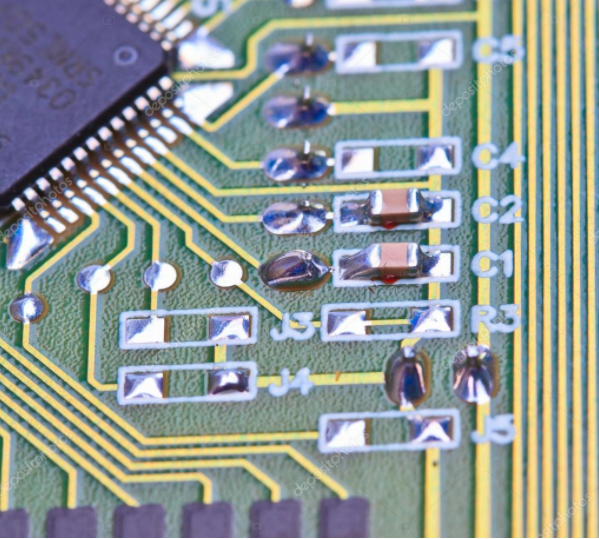
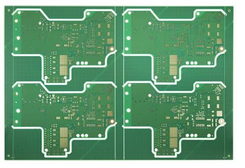
Vias are generally divided into three categories: through holes, blind holes and buried holes.
Blind hole: It is located on the top and bottom surfaces of the printed circuit board, with a certain depth, used for the connection of the surface circuit and the inner circuit below, the depth of the hole and the diameter of the hole usually do not exceed a certain ratio.
Buried hole: refers to the connection hole located in the inner layer of the printed circuit board, which does not extend to the surface of the circuit board.
Through hole: This kind of hole passes through the entire circuit board and can be used for internal interconnection or as a component installation positioning hole. Since through holes are easier to implement in process and lower cost, they are generally used on printed circuit boards.

Parasitic capacitance of via
The via itself has parasitic capacitance to ground. If the diameter of the isolation hole on the ground layer of the via is D2, the diameter of the via pad is D1, the thickness of the PCB is T, and the dielectric constant of the board substrate is ε, then The parasitic capacitance of the via is similar to:
C =1.41εTD1/(D2-D1)
The main effect of the parasitic capacitance of the via hole on the circuit is to prolong the rise time of the signal and reduce the speed of the circuit. The smaller the capacitance value, the smaller the effect.
Parasitic inductance of vias
The via itself has parasitic inductance. In the design of high-speed digital circuits, the harm caused by the parasitic inductance of the via is often greater than the influence of the parasitic capacitance. The parasitic series inductance of the via will weaken the function of the bypass capacitor and weaken the filtering effect of the entire power system. If L refers to the inductance of the via, h is the length of the via, and d is the diameter of the center hole, the parasitic inductance of the via is similar to:
L=5.08h[ln(4h/d) 1]
It can be seen from the formula that the diameter of the via has a small influence on the inductance, and the length of the via has the greatest influence on the inductance.
Via design in high-speed PCB
In high-speed PCB design, seemingly simple vias often bring great negative effects to circuit design. In order to reduce the adverse effects caused by the parasitic effects of the vias, the following can be done in the design:
(1) Choose a reasonable via size. For multi-layer general-density PCB design, it is better to use 0.25mm/0.51mm/0.91mm (drilled holes/pads/POWER isolation area) vias; for some high-density PCBs, 0.20mm/0.46 can also be used For vias of mm/0.86mm, you can also try non-through vias; for power or ground vias, you can consider using a larger size to reduce impedance;
(2) The larger the POWER isolation area, the better, considering the via density on the PCB, generally D1=D2+0.41;
(3) The signal traces on the PCB should not be changed as much as possible, that is to say, the vias should be reduced as much as possible;
(4) The use of a thinner PCB is conducive to reducing the two parasitic parameters of the via;
(5) The power and ground pins should be close to the vias. The shorter the lead between the vias and the pins, the better, because they will increase the inductance. At the same time, the power and ground leads should be as thick as possible to reduce impedance;
(6) Place some grounding vias near the vias of the signal layer to provide a short-distance loop for the signal.
the high-speed PCB In addition, the length of the via is also one of the main factors affecting the inductance of the via. For the via holes used for the top and bottom layers, the via length is equal to the PCB thickness. Due to the continuous increase in the number of PCB layers, the PCB thickness often reaches more than 5 mm. However, in high-speed PCB design, in order to reduce the problems caused by vias, the length of vias is generally controlled within 2.0mm. For vias with a length greater than 2.0 mm, the continuity of via impedance can be improved to a certain extent by increasing the aperture of the via. When the via length is 1.0 mm or less, the best via hole diameter is 0.20 mm-0.30 mm.