There are many inexperienced engineers in the electronics industry. The designed PCB boards often have various problems due to the neglect of certain inspections in the later stage of the design. Too close, signal loops, etc. As a result, electrical problems or process problems are caused, and the board must be re-printed in serious cases, resulting in waste. One of the most important steps in the later stage of PCB board design is inspection.
There are many details in the later inspection of PCB board design:
1. Component packaging
(1) Pad pitch
If it is a new device, draw the component package yourself to ensure that the spacing is appropriate. The pad spacing directly affects the soldering of the components.
(2) Via size (if any)
For plug-in devices, the size of the vias should be left with sufficient margin, generally not less than 0.2mm is more appropriate.
(3) Contour screen printing
The outline silk screen of the device should be larger than the actual size to ensure that the device can be installed smoothly.
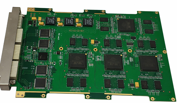
2. PCB board layout
(1) IC should not be near the edge of the board
(2) The components of the same module circuit should be placed close to each other
For example, the decoupling capacitor should be close to the power supply pin of the IC, and the components that make up the same functional circuit should be placed in one area with a clear hierarchy to ensure the realization of the function.
(3) Arrange the location of the socket according to the actual installation
Sockets are all lead to other modules. According to the actual structure, in order to facilitate installation, the principle of proximity is generally adopted to arrange the position of the socket, and it is generally close to the edge of the board.
(4) Pay attention to the direction of the socket
The sockets are oriented, and if the direction is reversed, the wire must be re-customized. For flat sockets, the direction of the socket should be toward the outside of the board.
(5) There can be no devices in the Keep Out area
(6) The source of interference should be far away from sensitive circuits
High-speed signals, high-speed clocks, or high-current switching signals are all interference sources and should be kept away from sensitive circuits, such as reset circuits and analog circuits. They can be separated by paving.
3. PCB board wiring
(1) Line width
The line width should be selected in combination with the process and the current carrying capacity, and the minimum line width should not be less than the minimum line width of the PCB board manufacturer. At the same time, the current carrying capacity is ensured, and the appropriate line width is generally selected at 1mm/A.
(2) Differential signal line
For differential cables such as USB and Ethernet, please note that the cables should be of equal length, parallel, and in the same plane, and the spacing is determined by the impedance.
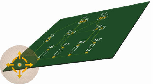
(3) Pay attention to the return path of the high-speed line
High-speed lines are prone to electromagnetic radiation. If the area formed by the routing path and the return path is too large, a single-turn coil will radiate electromagnetic interference outwards, as shown in Figure 1. Therefore, when wiring, pay attention to the return path next to it. The multi-layer board is provided with a power layer and a ground plane to effectively solve this problem.

Figure 1: PCB board design_reflow path of high-speed line
(4) Pay attention to the analog signal line
The analog signal line should be separated from the digital signal, and the wiring should be avoided to pass by interference sources (such as clocks, DC-DC power supply), and the wiring should be as short as possible.
4. Electromagnetic compatibility (EMC) and signal integrity of PCB board
(1) Termination resistance
High-speed lines or digital signal lines with higher frequencies and longer traces are best to have a matching resistor in series at the end.
(2) The input signal line is connected in parallel with a small capacitor
The signal line input from the interface should be connected to a small picofarad capacitor near the interface. The size of the capacitor is determined according to the strength and frequency of the signal, and cannot be too large, otherwise it will affect the signal integrity. For low-speed input signals, such as key input, a small capacitor of 330pF can be used, as shown in Figure 2.

Figure 2: PCB board design _ input signal line with small capacitor
(3) Driving ability
For example, a switching signal with a larger driving current can be driven by a triode; for a bus with a larger number of fan-outs, a buffer can be added.
5. The silk screen of PCB board
(1) Board name, time, PN code
(2) Label
Mark the pins or key signals of some interfaces (such as arrays).
(3) Component label
The component labels should be placed in a suitable position, and dense component labels can be placed in groups. Be careful not to place it in the position of the via.
6. Mark point of PCB board
For PCB boards that need to be welded by machine, two or three Mark points need to be added.