Anti-interference design principles for PCB board drawing
1. Ground wire layout:
1). The digital ground is separated from the analog ground.
2). The grounding wire should be as thick as possible, so that it can pass 3 times the allowable current on the printed board, and generally should be 2~3mm.
3). The grounding wire should form an endless loop as far as possible, so as to reduce the potential difference of the grounding wire.
2. Power cord layout:
1). According to the current size, try to widen the wire wiring.
2). The direction of the power cord and ground wire should be consistent with the direction of data transmission.
3). A decoupling capacitor of 10~100μF should be connected to the power input end of the printed board.
3. Decoupling capacitor configuration:
1). The lead wires of the decoupling capacitors should not be too long, especially the high frequency bypass capacitors should not have lead wires.
2). Connect a 10~100μF electrolytic capacitor across the power input end of the printed board, and it is better if it can be larger than 100μF.
3). Connect a 0.01~0.1μF ceramic capacitor between Vcc and GND of each integrated chip. If space is not allowed, a 1~10μF tantalum capacitor can be configured for every 4~10 chips.
4). Devices with weak anti-noise ability and large change in turn-off current, as well as ROM and RAM, should indirectly decoupling capacitors between Vcc and GND.
5). Match a 0.01μF decoupling capacitor on the reset terminal "RESET" of the microcontroller.
4. device configuration:
1). The clock input terminals of the clock generator, crystal oscillator and CPU should be as close as possible and far away from other low-frequency devices.
2). Keep small current circuits and high current circuits away from logic circuits as much as possible.
3). The position and direction of the printed board in the chassis should ensure that the device with a large amount of heat is on the top.
5. Separate the power line, AC line and signal line
The power line and AC line should be placed on a different board from the signal line as much as possible, otherwise they should be routed separately from the signal line.
6. Other principles:
1). When wiring, the address lines should be as long as possible and as short as possible.
2). Add a pull-up resistor of about 10K to the bus, which is beneficial to anti-interference.
3). The lines on both sides of the PCB should be arranged vertically as far as possible to prevent mutual interference.
4). The size of the decoupling capacitor is generally C=1/F, and F is the data transmission frequency.
5). Unused pins are connected to Vcc through a pull-up resistor (about 10K), or connected in parallel with the used pins.
6). Heat-generating components (such as high-power resistors, etc.) should avoid components that are easily affected by temperature (such as electrolytic capacitors, etc.).
7). The use of full decoding has stronger anti-jamming performance than line decoding.
In order to suppress the interference of high-power devices on the digital element circuit of the microcontroller and the interference of the digital circuit on the analog circuit, a high-frequency choke ring should be used when the digital ground and the analog ground are connected to a common ground point. This is a cylindrical ferrite magnetic material. There are several holes in the axial direction. A thicker copper wire is used to pass through the holes and wind one or two turns. This kind of device can be regarded as zero impedance for low-frequency signals., The interference to high-frequency signals can be regarded as an inductor.. (Because of the large DC resistance of the inductor, the inductor cannot be used as a high-frequency choke).
When signal wires other than the printed circuit board are connected, shielded cables are usually used. For high-frequency signals and digital signals, both ends of the shielded cable should be grounded. For shielded cables for low-frequency analog signals, one end should be grounded.
Circuits that are very sensitive to noise and interference or circuits that are particularly high-frequency noise should be shielded with a metal cover. The effect of ferromagnetic shielding on 500KHz high-frequency noise is not obvious, and the shielding effect of thin copper is better. When using screws to fix the shield, pay attention to the corrosion caused by the potential difference caused by the contact of different materials.
7. make good use of decoupling capacitors
The decoupling capacitor between the power supply of the integrated circuit and the ground has two functions: on the one hand, it is the energy storage capacitor of the integrated circuit, and on the other hand, it bypasses the high frequency noise of the device. The typical decoupling capacitor value in digital circuits is 0.1μF. The typical value of the distributed inductance of this capacitor is 5μH. The 0.1μF decoupling capacitor has a distributed inductance of 5μH, and its parallel resonance frequency is about 7MHz. That is to say, it has a better decoupling effect for noise below 10MHz, and it has little effect on noise above 40MHz.
Capacitors of 1μF and 10μF, and the parallel resonance frequency is above 20MHz, the effect of removing high-frequency noise is better.
Every 10 pieces of integrated circuits need to add a charge and discharge capacitor, or an energy storage capacitor, about 10μF can be selected. It is best not to use electrolytic capacitors. Electrolytic capacitors are rolled up with two layers of film. This rolled up structure behaves as an inductance at high frequencies. Use tantalum capacitors or polycarbonate capacitors.
The selection of decoupling capacitors is not critical, and C=1/F, that is, 0.1μF for 10MHz and 0.01μF for 100MHz.
When soldering, the pins of the decoupling capacitor should be as short as possible. Long pins will cause the decoupling capacitor itself to self-resonate. For example, the self-resonant frequency of a 1000pF ceramic capacitor with a pin length of 6.3mm is about 35MHz, and when the pin length is 12.6mm, it is 32MHz.

8. Experience in reducing noise and electromagnetic interference
Anti-jamming design principles of printed circuit boards:
1). A series of resistors can be used to reduce the jump rate of the upper and lower edges of the control circuit.
2). Try to make the potential around the clock signal circuit close to 0, circle the clock area with the ground wire, and the clock wire should be as short as possible.
3). The clock line perpendicular to the I/O line has less interference than the parallel to the I/O line.
4). The I/O drive circuit is as close as possible to the edge of the printed board.
5). Do not leave the output terminal of the gate circuit that is not in use. The positive input terminal of the unused operational amplifier should be grounded, and the negative input terminal should be connected to the output terminal.
6). Try to use 45° fold lines instead of 90° fold lines, wiring to reduce the external emission and coupling of high-frequency signals.
7). The pins of the component should be as short as possible.
8). Do not run wires under the quartz crystal or under components that are particularly sensitive to noise.
9). Do not form a current loop around the weak signal circuit and the ground wire of the low frequency circuit.
10). When necessary, add ferrite high-frequency choke to the circuit to separate signal, noise, power, and ground.
A via on the printed circuit board causes a capacitance of approximately 0.6pF; the packaging material of an integrated circuit itself causes a distributed capacitance of 2pF~10pF; a connector on a circuit board has a distributed inductance of 520μH; a dual in-line The 24-pin integrated circuit socket introduces 4μH~18μH distributed inductance.
Anti-jamming design of digital circuit and single-chip microcomputer
In the electronic system design, in order to avoid detours and save time, the anti-interference requirements should be fully considered and met, and anti-interference remedial measures should be avoided after the design is completed. There are three basic elements that cause interference:
1) Interference source refers to the component, equipment or signal that produces interference. It is described in mathematical language as follows: du/dt, the place where di/dt is large is the interference source. For example, lightning, relays, thyristors, motors, high-frequency clocks, etc. may all become interference sources.
2) Sensitive devices refer to objects that are easily disturbed. Such as: A/D, D/A converter, single chip microcomputer, digital IC, weak signal amplifier, etc.
3) Propagation path refers to the path or medium through which interference propagates from the interference source to the sensitive device. The typical interference propagation path is conduction through wires and radiation from space.
The basic principle of anti-interference design is to suppress the interference source, cut off the interference propagation path, and improve the anti-interference performance of sensitive devices. (Similar to the prevention of infectious diseases)
1. Suppress interference sources
Suppressing the interference source is to reduce the du/dt and di/dt of the interference source as much as possible. This is the best consideration and the most important principle in anti-jamming design, and it often has the effect of getting twice the result with half the effort. Reducing the du/dt of the interference source is mainly achieved by connecting capacitors in parallel at both ends of the interference source. Reducing the di/dt of the interference source is achieved by connecting inductance or resistance in series with the interference source loop and adding a freewheeling diode.
Common measures to suppress interference sources are as follows:
1) Avoid 90-degree fold lines when wiring to reduce high-frequency noise emission.
2) A freewheeling diode is added to the relay coil to eliminate the back-EMF interference generated when the coil is disconnected. Only adding a freewheeling diode will lag the off time of the relay. After adding a Zener diode, the relay can operate more times per unit time.
3) Connect a spark suppression circuit in parallel at both ends of the relay contact (usually an RC series circuit, the resistance is generally selected from a few K to tens of K, and the capacitor is 0.01uF) to reduce the impact of electric sparks.
4) Add a filter circuit to the motor, and pay attention to the shortest possible capacitor and inductance leads.
5) Each IC on the circuit board should be connected with a 0.01μF~0.1μF high frequency capacitor in parallel to reduce the IC's influence on the power supply. Pay attention to the wiring of high-frequency capacitors. The wiring should be close to the power supply terminal and as short as possible. Otherwise, the equivalent series resistance of the capacitor will be increased, which will affect the filtering effect.
6) Both ends of the thyristor are connected in parallel with the RC suppression circuit to reduce the noise generated by the thyristor (this noise may break down the thyristor). According to the propagation path of interference, it can be divided into two types: conducted interference and radiated interference.
The so-called conducted interference refers to the interference that propagates to sensitive devices through wires. The frequency bands of high-frequency interference noise and useful signals are different. You can cut off the propagation of high-frequency interference noise by adding a filter on the wire, and sometimes you can add an isolation optocoupler to solve it. Power noise is the most harmful, so pay special attention to handling. The so-called radiated interference refers to the interference that propagates to sensitive devices through space radiation. The general solution is to increase the distance between the interference source and the sensitive device, isolate them with a ground wire and add a shield on the sensitive device.
2. Common measures to cut off the interference propagation path are as follows:
1) Fully consider the impact of the power supply on the microcontroller. If the power supply is done well, the anti-interference of the whole circuit will be solved more than half. Many single-chip microcomputers are very sensitive to power supply noise. It is necessary to add a filter circuit or voltage regulator to the power supply of the single-chip microcomputer to reduce the interference of power supply noise to the single-chip microcomputer. For example, magnetic beads and capacitors can be used to form a π-shaped filter circuit. Of course, 100Ω resistors can be used instead of magnetic beads when the conditions are not high.
2) If the I/O port of the single-chip microcomputer is used to control noise devices such as motors, isolation should be added between the I/O port and the noise source (add a π-shaped filter circuit). To control noise devices such as motors, isolation should be added between the I/O port and the noise source (add a π-shaped filter circuit).
(3) Pay attention to the crystal oscillator wiring. The crystal oscillator is as close as possible to the pins of the microcontroller, the clock area is isolated with a ground wire, and the crystal oscillator shell is grounded and fixed. This measure can solve many difficult problems.
4) Reasonable division of the circuit board, such as strong and weak signals, digital and analog signals. Keep interference sources (such as motors, relays) away from sensitive components (such as single-chip microcomputers) as far as possible.
(5) Separate the digital area from the analog area with a ground wire, separate the digital ground from the analog ground, and finally connect it to the power ground at one point. The wiring of A/D and D/A chips is also based on this principle. Manufacturers have considered this requirement when assigning A/D and D/A chip pin arrangements.
(6) The ground wires of the single-chip microcomputer and high-power devices should be grounded separately to reduce mutual interference. Place high-power devices on the edge of the circuit board as much as possible.
(7) The use of anti-interference components such as magnetic beads, magnetic rings, power filters, and shields in key places such as the MCU I/O port, power cord, and circuit board connection line can significantly improve the anti-interference performance of the circuit.
3. Improve the anti-interference performance of sensitive devices
Improving the anti-interference performance of sensitive devices refers to the method of minimizing the pickup of interference noise from the side of sensitive devices and recovering from abnormal conditions as soon as possible.
Common measures to improve the anti-interference performance of sensitive devices are as follows:
(1) Minimize the loop loop area when wiring to reduce induced noise.
(2) When wiring, the power wire and ground wire should be as thick as possible. In addition to reducing the pressure drop, it is more important to reduce the coupling noise.
(3) For the idle I/O ports of the single-chip microcomputer, do not float, but should be grounded or connected to the power supply. The idle terminals of other ICs are grounded or connected to power without changing the system logic.
(4) The use of power supply monitoring and watchdog circuits for single-chip microcomputers, such as IMP809, IMP706, IMP813, X25043, X25045, etc., can greatly improve the anti-interference performance of the entire circuit.
(5) On the premise that the speed can meet the requirements, try to reduce the crystal oscillator of the single-chip microcomputer and select low-speed digital circuits.
(6) IC devices should be soldered directly on the circuit board as much as possible, and IC sockets should be used less.
Summary of experience
Software aspect:
1. It is used to clear all unused code spaces to "0", because this is equivalent to NOP, which can be returned when the program runs away;
2. Add several NOPs before the jump instruction, the purpose is the same as 1;
3. When there is no hardware WatchDog, software can be used to simulate WatchDog to monitor the operation of the program;
4. When dealing with the adjustment or setting of external device parameters, in order to prevent the external device from making errors due to interference, the parameters can be re-sent regularly, so that the external device can be restored as soon as possible;
5. Anti-interference in communication, data check digit can be added, and 3 out of 2 or 5 out of 3 strategies can be adopted;
6. When there is a communication line, such as I^2C, three-wire system, etc., in practice, we found that setting the Data line, CLK line, and INH line to high normally has better anti-interference effect than setting it to low.
Hardware aspect:
1. Wiring of ground wire and power wire
2. Decoupling of the line;
3. Separation of digital and modular ground;
4. Each digital component needs 104 capacitors between the ground and the power supply;
5. In order to prevent the crosstalk of the I/O port, the I/O port can be isolated by diode isolation, gate circuit isolation, photocouple isolation, electromagnetic isolation, etc.; 6. In applications with relays, especially high currents, to prevent the interference of relay contact sparks on the circuit, you can combine a 104 and a diode between the relay coils, and indirect 472 capacitors between the contacts and the normally open end, the effect is good!
7. Of course, the anti-interference of the multi-layer board is definitely better than that of the single-sided board, but the cost is several times higher.
8. Choosing a device with strong anti-interference ability is more effective than any other method. I think this should be the most important point. Because the inherent deficiencies of the components are difficult to make up for with external methods, but often the ones with strong anti-interference ability are more expensive, and the ones with poor anti-interference ability are cheaper, just like Taiwan's Dongdong is cheap but the performance is greatly reduced! It mainly depends on your application.
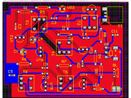
Printed circuit board (PCB) is the support of circuit components and devices in electronic products. It provides electrical connections between circuit elements and devices. With the rapid development of electrical technology, the density of PGB is getting higher and higher. The quality of PCB design has a great influence on the anti-interference ability. Therefore, in the PCB design. The general principles of PCB design must be followed, and the requirements of anti-interference design must be met.