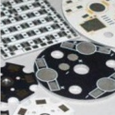
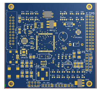
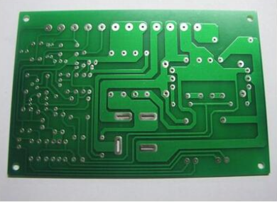
OC48 card layout
The high-speed analog signal between the optical transceiver and the DSP is very sensitive to external noise. Similarly, all special power supply and reference voltage circuits also cause a lot of coupling between the analog and digital power transmission circuits of the card. Sometimes, limited by the shape of the chassis, a high-density board has to be designed. Due to the location of the external optical cable access card and the relatively high size of the PCB components of the optical transceiver, the position of the transceiver in the card is largely fixed. The system I/O connector position and signal distribution are also fixed. This is the basic work that must be completed before layout.
Like most successful high-density analog layout and routing schemes, the layout must meet the routing requirements, and the layout and routing requirements must be balanced. For the analog part of a mixed-signal PCB and a local CPU core with a 2V operating voltage, it is not recommended to use the "layout before wiring" method. For the OC48 card, the DSP analog circuit part including the analog reference voltage and the analog power supply bypass capacitor should be interactively wired first. After completing the wiring, the entire DSP with analog components and wiring should be placed close enough to the optical transceiver to fully ensure that the wiring length from the high-speed analog differential signal to the DSP is the shortest, with the least bending and vias. The symmetry of the differential layout and routing will reduce the impact of common mode noise. However, it is difficult to predict the best plan for the layout before routing.

Consult the chip distributor for design guidelines for PCB layout. Before designing in accordance with the guidelines, it is necessary to fully communicate with the distributor's application engineer. Many chip distributors have strict time constraints on providing high-quality layout recommendations. Sometimes, the solutions they provide are feasible for "first-level customers" who use the device. In the field of signal integrity (SI) design, the signal integrity design of new devices is particularly important. According to the distributor’s basic guidelines and combined with the specific requirements of each power and ground pin in the package, you can begin to lay out and route the OC48 card with integrated DSP and microprocessor.
After the location and wiring of the high-frequency analog part are determined, the remaining digital circuits can be placed in accordance with the grouping method shown in the block diagram. Pay attention to carefully design the following circuits: the location of the PLL power filter circuit in the CPU with high sensitivity to analog signals; the local CPU core voltage regulator; the reference voltage circuit for the "digital" microprocessor.
The electrical and manufacturing guidelines for digital wiring can be properly applied to the design at this time. The aforementioned design of the signal integrity of the high-speed digital bus and clock signal reveals some special wiring topology requirements for the processor bus, balanced Ts, and time delay matching of certain clock signal wiring. But you may not know, some people have also put forward an updated suggestion, that is, to increase a number of termination resistors.
In the process of solving the problem, it is natural to make some adjustments in the layout stage. However, before starting wiring, a very important step is to verify the timing of the digital part in accordance with the layout plan. At this moment, a complete DFM/DFT layout review of the board will help ensure that the card meets the needs of customers.
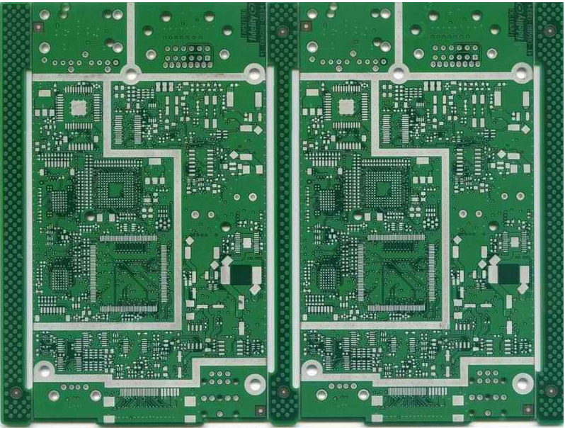
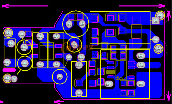
Digital wiring of OC48 card
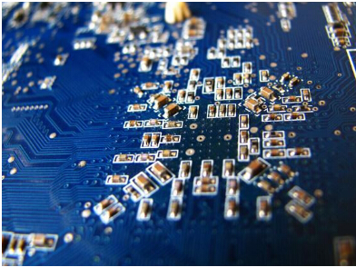
For the power lines of digital devices and the digital part of the mixed-signal DSP, the digital wiring should start from the SMD escape patterns. Use the shortest and widest printed line allowed by the assembly process. For high-frequency devices, the printed lines of the power supply are equivalent to small inductances, which will worsen power supply noise and cause undesired coupling between analog and digital circuits. The longer the power trace, the greater the inductance.
Using digital bypass capacitors can get the best layout and routing scheme. In short, fine-tune the position of the bypass capacitor as needed to make it easy to install and distribute it around the digital part and the digital part of the mixed-signal device. To use the same "shortest and widest trace" method to route the bypass capacitor.
When the power supply branch needs to pass through a continuous plane (such as the 3.3V power plane on the OC48 interface card), the power supply pin and the bypass capacitor itself do not have to share the same outlet diagram, and the lowest inductance and ESR bypass can be obtained. On mixed-signal PCBs such as the OC48 interface card, pay special attention to the wiring of the power supply branch. Remember to place additional bypass capacitors in a matrix arrangement on the entire card, and place the power supply even near the passive components. After the diagram is determined, you can start automatic routing. The ATE test contacts on the OC48 card should be defined during logic design. Make sure that ATE touches 100% of the nodes. In order to achieve ATE testing with the smallest ATE test probe of 0.070 inches, the position of the breakout via must be reserved to ensure that the power plane will not be interrupted by the cross of the antipads of the via.
If a power and ground plane split solution is to be used, a layer bias should be selected on the adjacent wiring layer parallel to the opening. Define the forbidden wiring area on the adjacent layer according to the perimeter of the opening area to prevent wiring from entering. If the wiring must pass through the open area to another layer, make sure that the other layer adjacent to the wiring is a continuous ground layer. This will reduce the reflection path. It is good for the layout of some digital signals to have bypass capacitors across the open power plane, but it is not recommended to bridge between the digital and analog power planes because noise will be coupled to each other through the bypass capacitors.
Several of the latest automatic routing applications are capable of routing high-density multi-layer digital circuits. In the initial wiring stage, use the 0.050-inch large-size via spacing in the SMD exit and consider the package type used. The subsequent wiring stage should allow the vias to be located closer to each other, so that all tools can achieve the highest layout rate. And the lowest number of vias. Because the OC48 processor bus uses an improved star topology, it has the highest priority during automatic routing.
After the completion of the OC48 card layout board, signal integrity verification and timing simulation are required. The simulation proves that the PCB wiring guidance meets the expected requirements and improves the timing indicators of the second-layer bus. Finally, the design rule check, the final manufacturing review, the mask and the review are issued to the manufacturer, and the layout task is officially ended.