As a professional manufacturer, PCB proofing manufacturers focus on the production and manufacture of PCB circuit boards. SMT chip processing, circuit board proofing, circuit board proofing, PCB board, circuit board factory, circuit board factory will take everyone to understand the PCB circuit board copy method and steps of PCB proofing.

The first step of PCB proofing is to get a piece. First, record the model, parameters, and positions of all vital parts on the paper, especially the direction of the diode, the direction of the three-machine tube, and the direction of the IC gap. It is best to use a digital camera to take two photos of the location of the vital parts.
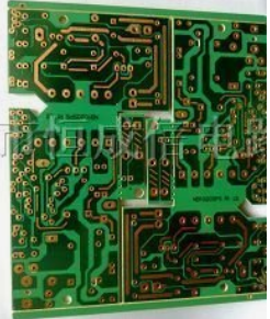
The second step of PCB proofing is to remove all the components and remove the tin in the PAD hole. Clean the PCB with alcohol, and then put it into the scanner. When the scanner scans, you need to raise the scanned pixels to get a clearer image. Start POHTOSHOP, scan the silk screen surface in color, and save the file And print it out for later use.
The third step of the PCB proofing is to lightly polish the TOP LAYER and BOTTOM LAYER with water gauze paper until the copper film is shiny, put it in the scanner, start PHOTOSHOP, and scan the two layers separately in color. Note that the PCB must be placed horizontally and straight in the scanner, otherwise the scanned image cannot be used, and the file should be saved.
The fourth step of PCB proofing is to adjust the contrast and brightness of the canvas to make the part with copper film and the part without copper film have a strong contrast, then turn the second image into black and white, and check whether the lines are clear. If not, repeat this step. If it is clear, save the picture as black and white BMP format files TOP.BMP and BOT.BMP. If you find any problems with the graphics, you can also use PHOTOSHOP to repair and correct them.
The fifth step of PCB proofing is to convert the two BMP format files into PROTEL format files, and transfer two layers in PROTEL. For example, the positions of PAD and VIA after the two layers basically coincide, indicating that the first few steps are well done. If there is a deviation, repeat the third step.
PCB proofing sixth, convert the BMP of the TOP layer to TOP.PCB, pay attention to the conversion to the SILK layer, which is the yellow layer, and then you can trace the line on the TOP layer, and place the device according to the drawing in the second step. Delete the SILK layer after drawing.
The seventh step of PCB proofing is to convert the BMP of the BOT layer to BOT.PCB, pay attention to the conversion to the SILK layer, which is the yellow layer, and then you can trace the line on the BOT layer. Delete the SILK layer after drawing.
The eighth step of PCB proofing is to import TOP.PCB and BOT.PCB in PROTEL, and it is OK to combine them into one picture.
The ninth step of PCB proofing is to use a laser printer to print the TOP LAYER and BOTTOM LAYER on the transparent film (1:1 ratio), put the film on the PCB, and compare whether there is an error. If it is correct, you can That's it.
Others: If it is a multi-layer board, you need to carefully polish the inner layer, and repeat the third to ninth steps. Of course, the naming of the graphics is also different. It depends on the number of layers. Generally, the double-sided board is better than the multi-layer board. The board is much simpler, and the multi-layer board copy board is prone to misalignment, so the multi-layer board copy board must be particularly careful and careful (where the internal vias and non-vias are prone to problems).