OSP is the abbreviation of (Organic Solderability Preservatives), which is translated as Organic Solderability Preservatives in Chinese, also known as Copper Protector, or Preflux in English. Its function is to block moisture, prevent oxidation of the pad, and maintain good solderability on the soldered copper surface. Due to the good surface flatness of OSP, high reliability of solder joints, relatively simple PCB manufacturing process and low cost, it has obvious advantages compared with other surface treatment PCBs, and it is more and more popular in the industry. Under normal circumstances, OSP surface treatment PCB has good tin properties, such as improper PCB production process control or improper use of SMT control will lead to poor soldering problems. According to the characteristics of OSP surface treatment PCB and poor soldering case analysis, this article focuses on the analysis of factors affecting PCB solderability from the aspects of OSP film thickness control, PCB storage and SMT use, and proposes some corresponding improvement measures.

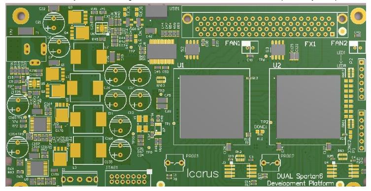
PCB is an indispensable material for modern electronic products. With the rapid development of surface mount technology (SMT) and integrated circuit (IC) technology, PCB needs to meet high density, high flatness, high reliability, smaller aperture, and smaller The requirements for the development of pads, the requirements for PCB surface treatment and manufacturing environment are also getting higher and higher. OSP surface treatment is currently a common PCB surface treatment technology. It is to chemically grow a 0.2~0.5um organic film on the clean bare copper surface. This film is anti-oxidation and resistant at room temperature. Thermal shock and moisture resistance can protect the copper surface from oxidation or sulfidation. In the subsequent high-temperature soldering, this protective film must be easily removed by the flux quickly, exposing a clean copper surface in a very short time Combine with molten solder to form a strong solder joint. Compared with other surface treatments, OSP surface treatment has the following advantages and disadvantages:
a. The OSP surface is flat and uniform, and the film thickness is 0.2~0.5um suitable for PCB with SMT close-pitch components;
b. OSP film has good thermal shock resistance, suitable for lead-free technology and single and double panel processing, and is compatible with any solder;
c. Water-soluble operation, the temperature can be controlled below 80 degree Celsius, will not cause the problem of substrate bending and deformation;
d. Good operating environment, less pollution, easy to automate the production line;
e. The process is relatively simple, the yield is high, and the cost is low;
f. The disadvantage is that the formed protective film is extremely thin, and the OSP film is easily scratched (or scratched);
g. After many times of high temperature soldering of the PCB, the OSP film (referring to the OSP film on the unsoldered pad) will undergo discoloration, cracking, thinning, and oxidation, which will affect the solderability and reliability;
h. There are many types of syrup formulas, different performances, and uneven quality.
2. Problem description
In the actual production process, OSP boards are prone to problems such as surface discoloration, uneven film thickness, and excessive film thickness (too thick or too thin); in the later stages of PCB production, the formed PCB is easy to appear if stored and used improperly Soldering problems such as oxidation of the pad, poor tin on the pad, inability to form a firm solder joint, virtual soldering and insufficient solder; SMT production of double-sided boards and soldering on the second side of the tin furnace are prone to poor reflow soldering, solder joint leakage, The appearance cannot meet the IPC3 level standard, and the soldering failure rate of the tin furnace is high.