With the development of power electronics technology, switching power supply modules have begun to replace traditional rectifier power supplies and are widely used in various fields of society due to their relatively small size, high efficiency, and reliable operation. However, due to the high operating frequency of the switching power supply, there are rapid current and voltage changes inside, namely dv/dt and di/dt, which will cause the switching power supply module to produce strong harmonic interference and spike interference, and through conduction, radiation and crosstalk Such coupling pathways affect the normal operation of its own circuit and other electronic systems, and of course it will also be affected by electromagnetic interference from other electronic equipment. This is the electromagnetic compatibility issue discussed, and it is also the electromagnetic disturbance EMD and electromagnetic susceptibility EMS design issue regarding the electromagnetic compatibility of the switching power supply. Since the country has begun to enforce 3C certification for some electronic products, whether an electronic device can meet electromagnetic compatibility standards will affect whether this product can be sold in the market, so it is very important to conduct electromagnetic compatibility research on switching power supplies.
Electromagnetic compatibility is a comprehensive subject, which involves theories including mathematics, electromagnetic field theory, antenna and radio wave propagation, circuit theory, signal analysis, communication theory, materials science, biomedicine, etc.
When designing the electromagnetic compatibility of the switching power supply, first carry out a system design and clarify the following points:
1. Clarify the electromagnetic compatibility standards that the system must meet;
2. Determine the key circuit parts in the system, including strong interference source circuits and highly sensitive circuits;
3. Identify the source of electromagnetic interference and sensitive equipment in the working environment of the power supply equipment;
4. Determine the electromagnetic compatibility measures to be taken for the power supply equipment.
One. Analysis of internal noise sources of DC/DC converters
1. The reverse recovery of the diode causes noise interference
Power frequency rectifier diodes, high frequency rectifier diodes, freewheeling diodes, etc. are often used in switching power supplies. Because these diodes are all working in the switching state, as shown in the figure, a Very high voltage spike VFP; there is a reverse recovery time trr during the diode's turn-on state to blocking operation. During the reverse recovery process, due to the existence of the diode package inductance and lead inductance, a reverse direction will occur. Voltage spike VRP, due to the storage and recombination effects of minority carriers, will produce transient reverse recovery current IRP. This rapid current and voltage sudden change is the root cause of electromagnetic interference.
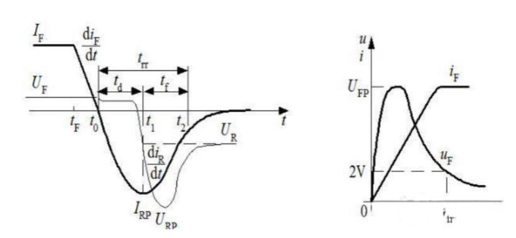
Current and voltage waveform
2. Electromagnetic interference occurs when the switch tube is switched on and off
The current and voltage waveform during diode reverse recovery The forward current and voltage waveform of diode
In forward, push-pull, and bridge converters, the current waveform flowing through the switch tube is similar to a rectangular wave under resistive load, and contains rich high-frequency components. These high-frequency harmonics will cause strong electromagnetic interference., In the flyback converter, the current waveform flowing through the switch tube is similar to a triangular wave when the resistive load is applied, and there are relatively few high-order harmonic components. When the switching tube is turned on, due to the short switching time and the existence of lead inductance in the inverter circuit, a large dV/dt mutation and high peak voltage will be generated. When the switching tube is turned off, the turn-off time is very long. Short, it will produce very big di/dt sudden change and very high current spike, these current, voltage sudden change will produce very strong electromagnetic interference.
3. Electromagnetic interference caused by magnetic components such as inductors and transformers: there are magnetic components such as input filter inductors, power transformers, isolation transformers, and output filter inductors in the switching power supply. There are parasitic capacitances between the primary and secondary stages of the isolation transformer, and high-frequency interference signals pass through the parasitic capacitances. Coupling to the secondary side; due to the winding process and other reasons, the power transformer has leakage inductance due to unsatisfactory primary and secondary side coupling. The leakage inductance will cause electromagnetic radiation interference. In addition, high-frequency pulse current flows through the coil windings of the power transformer, resulting in high-frequency surroundings. Electromagnetic field: The pulsating current flowing in the inductor will generate electromagnetic field radiation, and when the load suddenly cuts, it will form a voltage spike. At the same time, when it is working in a saturated state, it will produce a sudden current change, which will cause electromagnetic interference.
4. Periodic high-frequency pulse signals in the control circuit, such as the high-frequency pulse signals generated by the oscillator, will produce high-frequency and high-order harmonics, which will cause electromagnetic interference to the surrounding circuits.
5. In addition, there will be ground loop interference, common impedance coupling interference, and control power noise interference in the circuit.
6. The wiring design in the switching power supply is very important. Unreasonable wiring will cause electromagnetic interference to pass through the coupling capacitance and distributed mutual inductance between the wires or radiate to adjacent wires, thereby affecting the normal operation of other circuits.
7. Electromagnetic interference caused by thermal radiation. Thermal radiation is heat exchange in the form of electromagnetic waves. This electromagnetic interference affects the normal and stable operation of other electronic components or circuits.
2. External electromagnetic interference
For a certain electronic device, the electromagnetic interference caused by the outside world includes: harmonic interference in the power grid, lightning, solar noise, electrostatic discharge, and interference caused by surrounding high-frequency transmitting equipment.
Third, the consequences of electromagnetic interference
Electromagnetic interference will cause distortion of the transmission signal and affect the normal operation of the equipment. High-energy electromagnetic interference such as lightning and electrostatic discharge can damage the equipment in severe cases. For some devices, electromagnetic radiation can cause the leakage of important information.
Fourth, the electromagnetic compatibility design of the switching power supply
After understanding the internal and external electromagnetic interference sources of the switching power supply, we should also know that the three elements that form the electromagnetic interference mechanism are the propagation path and the disturbed equipment. Therefore, the electromagnetic compatibility design of the switching power supply mainly starts from the following three aspects: 1. Reduce the electromagnetic interference energy of the interference source; 2. Cut off the interference propagation path; 3. Improve the anti-interference ability of the disturbed device.
It is very important to correctly understand and grasp the electromagnetic interference source of the switching power supply and its generation mechanism and interference propagation path for the anti-interference measures to be taken to make the equipment meet the electromagnetic compatibility requirements. Since the interference source has the interference source generated inside the switching power supply and the external interference source, and it can be said that the interference source cannot be eliminated, and the disturbed device always exists, so it can be said that the electromagnetic compatibility problem always exists.
The following takes the isolated DC/DC converter as an example to discuss the electromagnetic compatibility design of the switching power supply:
1. Design of DC/DC converter input filter circuit
As shown in the figure, FV1 is a transient voltage suppression diode, and RV1 is a varistor. Both have strong transient surge current absorption capacity, which can protect the subsequent components or circuits from surge voltage damage. . Z1 is a DC EMI filter, it must be well grounded, the grounding wire should be short, it is best to install it directly on the metal shell, and the shielding isolation between the input and output wires must be ensured to effectively cut off the propagation of conducted interference along the input wire. And radiation interference spreads along the space. L1 and C1 form a low-pass filter circuit. When the inductance of L1 is large, the V1 and R1 components as shown in the figure should be added to form a freewheeling loop to absorb the electric field energy released when L1 is disconnected, otherwise the voltage spike generated by L1 Electromagnetic interference will be formed. The magnetic core used by the inductor L1 is preferably a closed magnetic core. The leakage magnetic field of the open-loop magnetic core with an air gap will cause electromagnetic interference. The capacity of C1 is better, so that the input line can be reduced. The ripple voltage on the input wire, thereby reducing the electromagnetic field formed around the input wire.
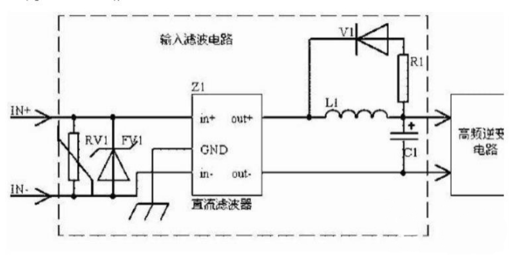
DC/DC converter input filter circuit
2. The electromagnetic compatibility design of the high frequency inverter circuit, as shown in the figure, the half-bridge inverter circuit composed of C2, C3, V2, and V3, V2 and V3 are switching elements such as IGBT and MOSFET, which are turned on and off at V2 and V3 When off, due to the fast switching time and the presence of lead inductance and transformer leakage inductance, the loop will produce higher di/dt and dv/dt mutations, which will cause electromagnetic interference. For this reason, R4 and C4 are added at both ends of the primary side of the transformer. To form an absorption loop, or connect capacitors C5 and C6 in parallel at both ends of V2 and V3, and shorten the lead to reduce the lead inductance of ab, cd, gh, and ef. In the design, C4, C5, and C6 generally use low-inductance capacitors. The size of the capacitor depends on the lead inductance, the current value in the loop and the allowable overshoot voltage value. The formula LI2/2=C△V2/2 Get the size of C, where L is the loop inductance, I is the loop current, and △V is the overshoot voltage value.
In order to reduce △V, it is necessary to reduce the loop lead inductance. For this reason, a device called "multi-layer low-inductance composite busbar" is often used in the design. The inductance is reduced to a sufficiently small level, up to 10nH, so as to achieve the purpose of reducing the electromagnetic interference of the high-frequency inverter loop.
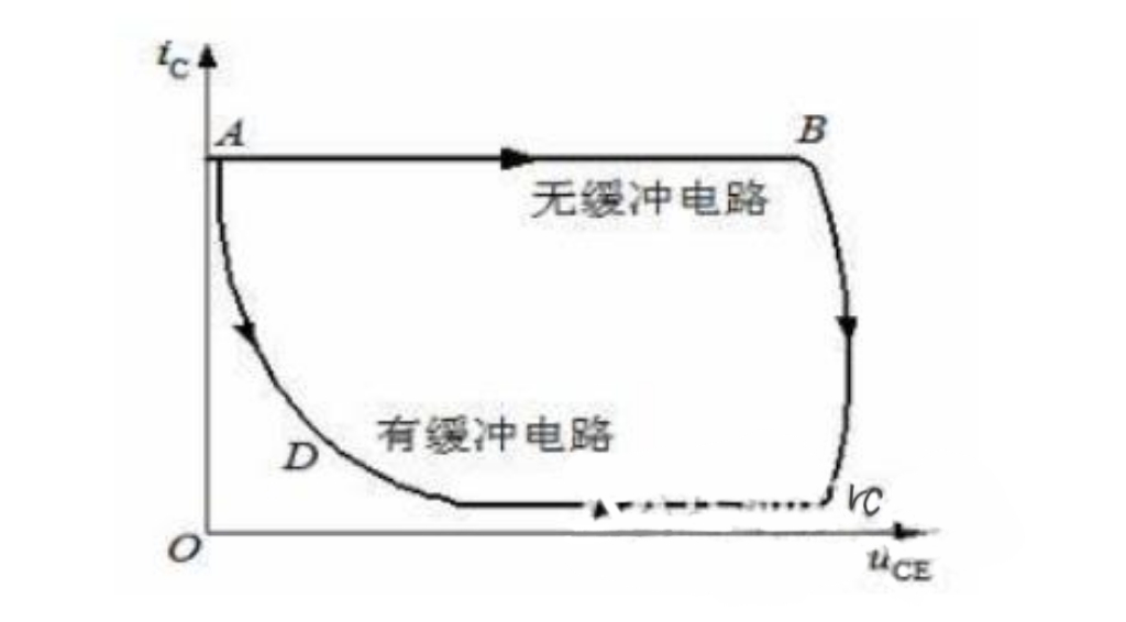
Comparison chart of switching tube current and voltage waveforms
From the perspective of electromagnetic compatibility design, the switching frequency of the switching tubes V2 and V3 should be reduced as much as possible, thereby reducing the di/dt and dv/dt values. In addition, the use of ZCS or ZVS soft switching technology can effectively reduce the electromagnetic interference of the high-frequency inverter loop. The fast switching action under high current or high voltage is the root of electromagnetic noise. Therefore, choose a circuit topology that produces less electromagnetic noise as much as possible. For example, under the same conditions, a two-tube forward topology is more likely to produce electromagnetic noise than a single-tube forward topology. Small, the full-bridge circuit generates less electromagnetic noise than the half-bridge circuit.
From the perspective of electromagnetic compatibility design, the switching frequency of the switching tubes V2 and V3 should be reduced as much as possible, thereby reducing the di/dt and dv/dt values. In addition, the use of ZCS or ZVS soft switching technology can effectively reduce the electromagnetic interference of the high-frequency inverter loop. The fast switching action under high current or high voltage is the root of electromagnetic noise. Therefore, choose a circuit topology that produces less electromagnetic noise as much as possible. For example, under the same conditions, a two-tube forward topology is more likely to produce electromagnetic noise than a single-tube forward topology. Small, the full-bridge circuit generates less electromagnetic noise than the half-bridge circuit.
As shown in the figure, the current and voltage waveforms on the switch tube after the absorption circuit is added are compared with the waveforms without the absorption circuit.
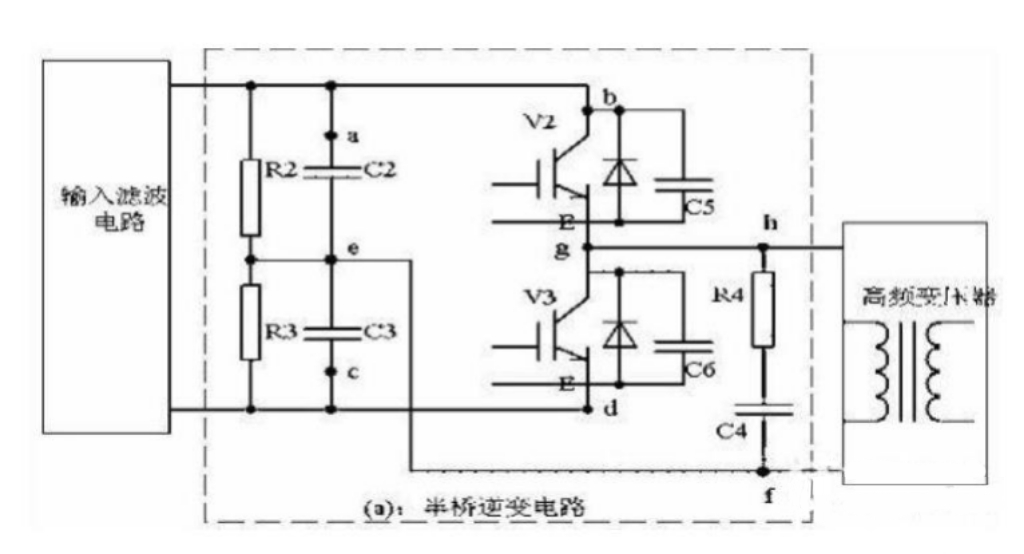
Half-bridge inverter circuit
3. EMC design of high frequency transformer
When designing high frequency transformer T1, try to choose magnetic core material with better electromagnetic shielding performance.
As shown in the figure, C7 and C8 are inter-turn coupling circuits, and C11 is the inter-winding coupling capacitor. When winding the transformer, minimize the distributed capacitor C11 to reduce the coupling of high-frequency interference from the primary side of the transformer to the secondary winding. In addition, in order to further reduce electromagnetic interference, a shielding layer can be added between the primary and secondary windings, and the shielding layer is well grounded, so that coupling capacitors C9 and C10 are formed between the primary and secondary windings of the transformer and the shielding layer, and high-frequency interference currents pass C9 and C10 flow to the earth.
Since the transformer is a heating element, poor heat dissipation conditions will inevitably lead to an increase in the temperature of the transformer, thereby forming heat radiation. The heat radiation is transmitted in the form of electromagnetic waves. Therefore, the transformer must have good heat dissipation conditions.
Usually the high frequency transformer is encapsulated in an aluminum shell box. The aluminum box can also be installed on an aluminum radiator and filled with electronic silica gel, so that the transformer can form a better electromagnetic shield and ensure a better heat dissipation effect. Reduce electromagnetic radiation.
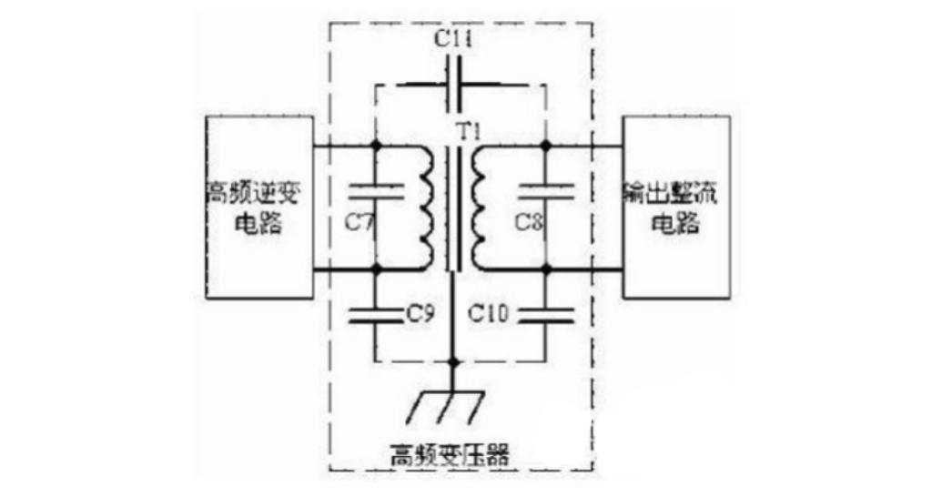
EMC Design of High Frequency Transformer
5. EMC design of output rectifier circuit
The figure shows the output half-wave rectifier circuit, V6 is a rectifier diode, and V7 is a freewheeling diode. Since V6 and V7 work in high-frequency switching states, the electromagnetic interference sources of the output rectifier circuit are mainly V6 and V7, R5, C12 It is connected with R6 and C13 to form the absorption circuit of V6 and V7 respectively, which is used to absorb the voltage spikes generated during the switching operation and dissipate it in the form of heat on R5 and R6.
Reducing the number of rectifier diodes can reduce the energy of electromagnetic interference. Therefore, under the same conditions, the use of half-wave rectification circuits will produce less electromagnetic interference than the use of full-wave rectification and full-bridge rectification.
In order to reduce the electromagnetic interference of the diode, a diode device with soft recovery characteristics, small reverse recovery current and short reverse recovery time must be selected. Theoretically speaking, Schottky barrier diodes (SBD) conduct majority carrier current, and there is no storage and recombination effect of minority carriers, so there will be no reverse voltage spike interference. For Schottky diodes with operating voltages, as the thickness of the electronic barrier increases, the reverse recovery current will increase, and electromagnetic noise will also be generated. Therefore, when the output voltage is low, the electromagnetic interference generated by choosing Schottky diodes as DC diodes will be smaller than choosing other diode devices.
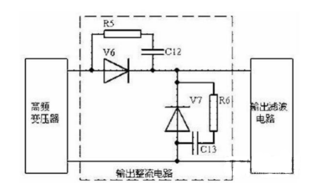
Electromagnetic compatibility design of output rectifier circuit
6. EMC design of output DC filter circuit
output DC filter circuit is mainly used to cut off the propagation of electromagnetic conduction interference along the wire to the output load end, and reduce the electromagnetic radiation of electromagnetic interference around the wire.
As shown in the figure, the LC filter circuit composed of L2, C17, and C18 can reduce the size of the output current and voltage ripple, thereby reducing the electromagnetic interference transmitted through radiation. The filter capacitors C17 and C18 should be connected in parallel with multiple capacitors as much as possible. Reduce the equivalent series resistance, thereby reducing the ripple voltage. The output inductance L2 should be as large as possible to reduce the size of the output ripple current. In addition, it is better to use a closed-loop magnetic core with no air gap for the inductance L2, preferably not a saturated inductance. . When designing, we must remember that there are changes in current and voltage on the wire, and there is a changing electromagnetic field around the wire, and the electromagnetic field will spread along the space to form electromagnetic radiation.
C19 is used to filter the common mode interference on the wire, try to use low-inductance capacitors, and the wiring should be short, C20, C21, C22, C23 are used to filter the differential mode interference on the output line, and low-inductance three-terminal capacitors should be used, And the grounding wire should be short and reliable.
Z3 is a DC EMI filter. It is used or not according to the situation, whether it is a single-stage or multi-stage filter. However, it is required that Z3 be directly installed on a metal chassis. It is best that the input and output lines of the filter can be shielded and isolated.
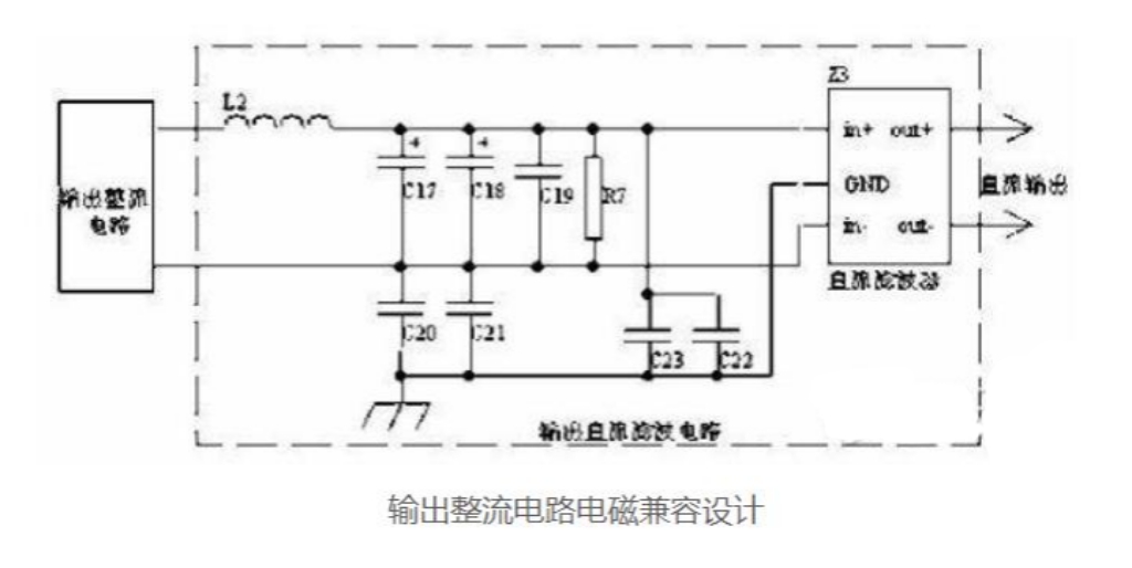
Electromagnetic compatibility design of output rectifier circuit
7. Electromagnetic compatibility design of contactors, relays and other switching devices
After the power of relays, contactors, fans, etc., their coils will produce larger voltage spikes, which will cause electromagnetic interference. For this reason, connect a diode or RC absorption circuit in parallel at both ends of the DC coil, and connect a parallel at both ends of the AC coil. The varistor is used to absorb the voltage spike generated after the coil is powered off. At the same time, it should be noted that if the contactor coil power supply and the auxiliary power input power supply are the same power supply, it is best to pass an EMI filter between them. Electromagnetic interference will also be generated when the relay contacts are in action, so RC absorption loops should be added at both ends of the contacts.
8. The electromagnetic compatibility design of the switch power supply box structure
Material selection: There is no "magnetic insulation" material. Electromagnetic shielding uses the principle of "magnetic short circuit" to cut off the propagation path of electromagnetic interference inside the device and in the outside air. When designing the cabinet structure of the switching power supply, it is necessary to fully consider the impact on electromagnetic interference
Shielding effectiveness, the principle of selection of shielding materials is that when the frequency of the interference electromagnetic field is high, high-conductivity metal materials are used, and the shielding effect is better; when the frequency of the interference electromagnetic wave is low, high-permeability metal materials should be used, The shielding effect is better; in some occasions, if a good shielding effect is required for both high-frequency and low-frequency electromagnetic fields, metal materials with high conductivity and high permeability are often used to form a multilayer shield.
Hole, gap, overlap treatment method: The electromagnetic shielding method does not need to redesign the circuit, and a good electromagnetic compatibility effect can be achieved. The ideal electromagnetic shielding body is a conductive continuum with no gaps, no holes, no penetration, and a low-impedance metal sealing body, but a completely sealed shielding body is of no practical value, because in the switching power supply equipment, there is input, Output line through holes, heat dissipation vents and other holes, as well as the overlapping gaps between the structural components of the box, if no measures are taken, electromagnetic leakage will occur, which will reduce the shielding effectiveness of the box or even completely lose it. Therefore, in the design of the switching power supply box, it is best to use welding for the overlap between the metal plates. When welding is not possible, use electromagnetic gaskets or other shielding materials. The openings on the box should be smaller than the wavelength of the electromagnetic wave to be shielded. 1/2, otherwise the shielding effect will be greatly reduced; for the ventilation holes, perforated metal plates or metalized wire mesh can be used when the shielding requirements are not high, and the cut-off waveguide should be used when high shielding efficiency and good ventilation effect are required. And other methods to improve the shielding effectiveness of the shield. If the shielding effectiveness of the box still cannot meet the requirements, you can spray shielding paint on the box. In addition to shielding the entire cabinet of the switching power supply, it can also partially shield the internal components and parts of the power supply equipment such as interference sources or sensitive equipment.
When designing the cabinet structure, design a low-impedance current discharge path for all parts of the equipment that will be subjected to the electrostatic discharge test. The cabinet must have reliable grounding measures and ensure the current-carrying capacity of the grounding wire. At the same time, keep sensitive circuits or components away from these bleeder circuits, or use electric field shielding measures for them. For the surface treatment of structural parts, electroplating of silver, zinc, nickel, chromium, and tin is generally used. This requires consideration of electrical conductivity, electrochemical reaction, cost, and electromagnetic compatibility.
9.EMC design in component layout and wiring:
The layout of the internal components of the switching power supply equipment must consider the requirements of electromagnetic compatibility as a whole. The interference sources inside the equipment will affect the operation of other components or components through radiation and crosstalk. Research has shown that at a certain distance from the interference source, the interference The energy of the source will be greatly attenuated, so a reasonable layout will help reduce the influence of electromagnetic interference.
It is best to install the EMI input and output filter at the entrance of the metal chassis, and ensure that the input line and the output line are shielded and isolated from the electromagnetic environment.
Keep sensitive circuits or components away from heat sources.