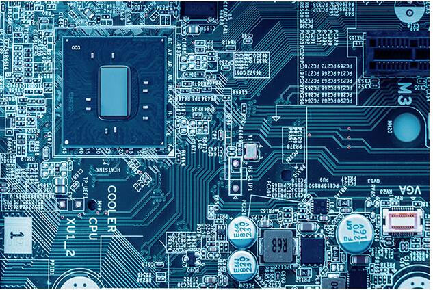
1. FPC imposition design process requirements
SMT processing practice proves that the imposition size of FPC should not be too large, and the normal imposition is 250mm*200mm (for small devices with only capacitors, resistors, and inductances). If the FPC is mounted with ICs and headphones. For motors, USB ports, and connectors with large PIN numbers, it’s best to control the imposition size within 250mm*150mm, because the larger the board, the greater the expansion and contraction of the FPC. For SMT processing and printing solder paste, the FPC will not be printed. On the pad. While considering the efficiency and quality yield of SMT processing and production, the following issues should be paid attention to.
1.1. The plate size and the number of impositions must fully consider the overall production efficiency.
1.2. Design requirements for positioning holes and optical identification points on the FPC.
The positioning hole (SMT positioning hole) and the optical recognition alignment point (SMT alignment recognition point) on the FPC need to meet the accuracy requirements of solder paste printing and placement. Because they directly affect the quality of FPC printing solder paste and placement. The positioning difference is controlled within 0.1mm. At the same time, the positioning holes and alignment points of each board must be consistent.

1.3. The reinforcement board for FPC structure selection is the focus of the evaluation.
The number of layers and structure of the FPC substrate, the material selection and thickness requirements of the reinforcement board, and the connection point process are an important part of the evaluation of the SMT process of the imposition evaluation. They greatly affect the yield of FPC SMT assembly and the reliability of FPC devices after soldering.
1. Requirements for surface treatment process of FPC device pads.
2.1 ENEG process of electroplating nickel gold.
2.2. ENIG technology for learning insurance gold. The influence of the abnormality of the nickel-gold pad on the SMT processing and welding can refer to the analysis of the abnormal soldering caused by the ENIG pad in the "Modern Surface Mount Information" and the rework method
2.3. Organic protective film (OSP) process.
The above three processes are common pad treatment processes for FPC, and each has its own advantages and disadvantages.
The choice of pad surface treatment process also determines the reliability of soldering. For example, nickel gold is prone to produce "black pads" which directly affect the solderability of SMT. The OSP process has high requirements for the production of FPC before SMT. The film is easily oxidized, which is fatal to SMT soldering. . For details, please refer to the research on the solderability of different surface treatments of BGA in the SMT process in the 6th issue of "Modern Surface Mount Information" in December 2012. 3. The solder mask design requirements of FPC pads.
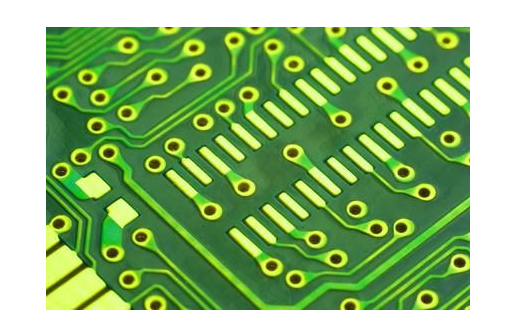
The solder mask on the FPC (SolderMask) is similar to the "green oil" on the PCB. The difference is that the green oil on the PCB is silk-screened, while the solder mask on the FPC is made by the following two methods: This is a polyimide film as the material. The windowing system is formed by drilling and punching the die, and then pressed with the main board to form the window of the pad. The other is the same as the green oil on the PCB. No matter what kind of "windowing" method is adopted. For the SMD/SMC device pads, ensure that the pads are uniform and symmetrical, and the pads cannot be covered by the solder mask
Poor pads on the solder mask will reduce the solderable area of the SMT during soldering, which will lead to failure of reliability after soldering.
There are two main ways to open windows in SMD/SMC pad design: one is SMD (Solder Mask Defined) solder mask limitation, and the other is NSMD (Non-Solder Mask Defined) non-solder mask defined.
The above are the 4 windowing methods for SMD/MSC pads. Now it uses NSMDPAD and NSMD to open the window. For these two window opening methods, the overlay film and the green oil solder mask are required to be aligned.
4. The design rationality of SMD/SMC pads affects SMT processing.
4.1. The device pad design is designed according to the customer's original window opening, and there will be defects in SMT processing.
4.2. The matching of the pads on the FPC flexible printed circuit board and the soldering feet of the SMD/SMC devices has an impact on the SMT processing and soldering.
4.2.1. The pad on the FPC flexible printed circuit board is smaller than the solder foot of the SMD/SMC device, and the SMT cannot be soldered.
4.2.2. The inner distance of the pads on the FPC flexible printed circuit board is too large. The excessive inner distance of the pads on the FPC flexible printed circuit board causes the solder feet of the SMD/SMC devices to fail to lay on the pads, which directly causes the SMT to fail to be soldered.
4.3. Whether the solder feet of the SMD/SMC device match the pads of the corresponding SMD/SMC device on the FPC.
In the design process of FPC, it is necessary to consider the matching of the solder feet of the SMD/SMC device and the corresponding SMD/SMC device on the FPC. For example, the FPC requires the mounting of 0402 devices, but the design of the pad on the FPC is in accordance with the 0603 pad specification To design. In this way, it is impossible to solder in SMT. Either replace the 0603 specification device, or adjust the pad design on the FPC.