With the rapid development of computer-led circuit signal transmission, one of the most important issues is that the PCB is required to maintain signal stability during high-speed signal transmission without malfunction, which requires the characteristic impedance of the PCB used. Improved control accuracy. Put forward more stringent requirements on the accuracy of characteristic impedance control, which is indeed a great challenge for PCB manufacturers. Therefore, this article discusses how to meet the strict impedance control accuracy requirements of customers. Colleagues are helpful.
1 Introduction
With the rapid development of electronic products, this requires the characteristic impedance control of the PCB used to achieve high precision. Taking the progress of high-speed computers as an example, it can illustrate the development trend of this demand.

Initially, the ±10% control accuracy requirement for PCB was established by the application of Direc Rambus DRAM module (RIMM) with 800MHz frequency signal in the circuit. This is to ensure that the internal circuit of the computer host and the switch achieves higher speed operations. Not only are computer products equipped with RIMM, but many electronic products also require the circuit on the substrate to be well matched. The characteristic impedance control accuracy of the PCB boards used by some customers is not limited to the original ±15% or ±10. %, some impedance control accuracy requirements are increased to ±8% or even ±5%, which is indeed a great challenge for PCB manufacturers. This article mainly focuses on how to meet customers' strict impedance control accuracy requirements, and hopes to be helpful to PCB manufacturing counterparts.
2. Impedance control precision analysis
Generally, it is easy for the transmission line system of the multilayer board to reach 60±10%Ω, but it is a bit difficult to reach 75±5%Ω, or even 50±5%Ω. The error of 5% is even for those with higher technical specifications. It is not common in application, but there are still some customers who have put forward the requirement of ±5% for impedance control accuracy. Here is an example to illustrate.
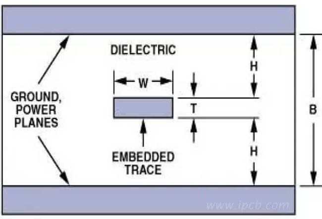
The following is a kind of board produced by our company. The requirements of the board: 4-layer board, finished board thickness 1.0±0.10mm, board adopts FR4, customer has specified laminated structure, see the figure below

2.1 Simulation calculation of PCB characteristic impedance
For boards with impedance control requirements, at present, a common practice in PCB factories is to design some impedance samples at appropriate positions on the side of the PCB production imposition board. These impedance samples have the same layering and impedance line structure as the PCB. Before designing the impedance sample, some impedance calculation software will be used to simulate the impedance in advance in order to predict the impedance. Among them, the CITS test system and calculation software developed by the British POLAR company have been used by many PCB manufacturers since 1991, and they are simple to operate and have powerful functional computing capabilities. However, no matter how powerful the system is, its computing power and field solving tools for calculating impedance all rely on the use of "ideal" materials, and there will always be a certain deviation between the results of simulation calculations and the actual measured impedance results. Therefore, when the customer's impedance control accuracy is required to be ±5%, it is particularly important to use software with higher calculation accuracy to carry out more accurate simulation prediction. To this end, we use the latest calculation software Polar SI8000K controlled impedance fast solver developed by the British POLAR company to simulate and predict. Due to customer requirements: in order to meet the impedance of 50±5%Ω, the PCB factory can make appropriate adjustments to the laminated structure. The impedance line width cannot be adjusted. For this reason, the simulation results are as follows:

2.2 PCB production process control
2.2.1 Production with parallel light exposure machine
Because non-parallel light belongs to a point light source, the emitted light is scattered light. Therefore, these rays of light enter the photosensitive dry film or other liquid anti-etchant film through the film negative and are exposed at various angles, and are exposed and developed. There will be a certain deviation between the pattern and the pattern on the negative. The parallel light is irradiated to the photosensitive dry film or other liquid resist film in the vertical direction for exposure. Therefore, the width of the exposed wire on the photosensitive layer will be very close. The width of the wire on the film negative, in this way, can get a more accurate wire width, thereby reducing the impact of this deviation on impedance.
2.2.2 Use thin copper foil for outer base copper
Due to the rapid development of fine circuits, thin copper foil has been extensively developed and fully used. The thickness of copper foil has been mainly from 1OZ to 1/2OZ in the early years, and 1/3OZ and 1/4OZ have also been developed. Even thinner ones such as 1/7OZ copper foil. Because the thinner copper foil thickness is conducive to manufacturing and controlling the width of the wire and the integrity of the wire, thereby helping to ensure the accuracy of impedance control. Since the customer's outer layer copper thickness is 1OZ, we chose 1/3OZ copper foil for the outer layer of the four-layer board. After the subsequent electroplating, it can reach the customer's surface copper thickness of 1OZ copper. Thickness requirements, which not only meets the customer's requirements for the copper thickness on the surface, but also facilitates the control of the uniformity of the wire width during etching.
2.2.3 Laminating with copper foil energized heating press
The heating method of the laminator is electric heating and steam heating, and our company uses a multi-layer vacuum press produced by CEDAL, Italy, which adopts ADARA technology. The system uses a rolled copper foil to surround the prepreg and inner layer. The board is laminated one by one. The copper foil is energized in the laminator to achieve the heating effect and temperature distribution. The temperature distribution of the entire laminated board can reach 177±2°C. Due to the fast heating, the temperature distribution is even. During the pressing process, the resin fluidity is relatively uniform, the thickness and flatness of the laminated board can reach ±0.025mm, and the thickness of the interlayer dielectric layer is relatively uniform.
2.2.4 Production using whole plate electroplating
In order to obtain a relatively uniform thickness and width of the wire to ensure that the impedance is within the specified tolerance range, the PCB is directly produced by full-board electroplating after the holeization, in which the current density is appropriately reduced. Because the PCB enters directly after the holeization Full-plate electroplating, under certain plating solution conditions, the entire plate surface receives a uniform current density, so the copper thickness of the entire plate surface and the hole is relatively uniform, which is beneficial to control the surface copper thickness and The uniformity of the wire width (because the uneven copper thickness will bring disadvantages to the uniformity of etching), which is beneficial to the control of the characteristic impedance of the PCB and the reduction of its volatility.
2.2.5 Other aspects
Of course, in order to meet the customer's 50±5%Ω (50±2.5Ω) impedance control requirements, etching lines and silk screen green oil should also be controlled to ensure the uniformity of the wire width and the thickness of the green oil layer on the wire surface.
2.3 Impedance measurement of PCB
Impedance measurement is usually done using a time domain reflectometer (TDR), and TDR (time domain reflectometer) has become an established technique for measuring the characteristic impedance on a printed circuit board. The impedance measurement is also very important for the characteristic impedance with an accuracy of ±5%. It is necessary to ensure the accuracy of the measurement, otherwise it will cause the board with qualified impedance to be falsely detected as unqualified.
2.3.1 Use traceable impedance standards for calibration before measurement
Because the TDR used for impedance measurement is a high-precision RF measurement tool, during the measurement process, the TDR measurement must be performed under the same DC conditions at the front end and the back end of the trace. Since most of the impedance COUPON is not terminated, Therefore, it is best to use a reference air line that has been calibrated to a traceable standard. Using high-precision load resistance to calibrate TDR can reduce impedance measurement errors
2.3.2 Do not place your hands on the impedance COUPON during measurement
When the hand or finger is placed on the impedance COUPON, the impedance structure of the surface changes, which results in a decrease in the measured impedance. For this reason, the tester should not put his hands or fingers on the impedance COUPON during the test.
2.3.3 Use a fixed test fixture to fix the impedance COUPON during testing
The usual way to test impedance is to place the impedance COUPON directly on the work surface for testing. This will affect the measurement result, because the work surface has its own insulation constant. If the impedance COUPON is in direct contact with the work surface, the impedance test result will be obtained. Of course, the impedance control accuracy requirements are not very strict. However, when testing the characteristic impedance with an accuracy of ±5% for similar measurement impedance, a fixed test fixture should be used to test the impedance COUPON.
2.3.4 Check the RF cable and probe wear during measurement
The service life of RF cables and probes is limited, and users will wear out during use. Once the RF cables and probes are damaged, it will affect the impedance measurement results. Therefore, check the wear of the RF cables and probes during measurement to ensure that the measurement is ensured. The correctness.
2.3.5 Other aspects
Of course, in order to ensure the accuracy of the measurement, the mobile phone near the test area is required to be closed during the measurement process, and the TDR impedance test probe is required to ensure good contact with the impedance test COUPON during the measurement.
3. Results and discussion
The following is the impedance test result of the board tested by the TDR test system. It can be seen from the result that the impedance tested by the board is between 47.5∽52.5Ω, which fully meets the customer’s 50±5%Ω (50±2.5Ω) Impedance requirements. Therefore, it can be seen that for the customer's impedance control accuracy requirements of ±8% or even ±5%, as long as the software with higher calculation accuracy is used for more accurate simulation prediction before production, and the results of simulation prediction are combined with the corresponding parameters Make appropriate adjustments to give special control to key processes in the production process. At the same time, it is still achievable to ensure the accuracy of the measurement during measurement.