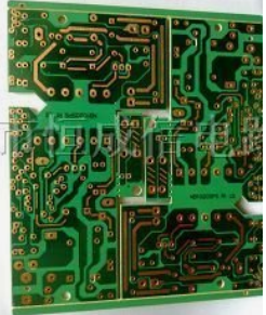
Explain to everyone why there are many small holes on the PCB:
The small holes on the PCB are vias, which are used to connect the electrical signals of one layer to another layer. The holes on the PCB board can be roughly divided into three types, screw holes, conductive holes, and plug-in holes.

The screw holes are used for fixing.
Conductive holes (also called vias) are used to conduct electricity just like wires.
The plug-in hole is of course used to insert various parts, such as diodes, triodes, capacitors, inductors and the like.
PCB is divided into single-sided board, double-sided board, and more, and the board with more than double-sided should be connected from one side to the other side with conductive holes.
1. Some net lines must be punched on the two layers
2. Two layers of large-area ground GND, with many holes, can reduce noise and buffer the deformation of the circuit board.
Those are vias, which are used to connect electrical signals from one layer to another.
To add, the kid is usually a via, which not only plays a role in conduction, but many reasons are that it can reduce the parasitic capacitance caused by copper and platinum on both sides, which means to eliminate the effect of parasitic capacitance, and the other is to increase the conduction rate.. ....
The holes in the PCB are divided into PTH and NPTH holes, namely through holes and non-through holes. The through holes play the role of conduction between the layers after the immersion copper board is electrically connected, that is, the first layer line and the second layer line Conductive and non-conductive holes are divided into positioning holes and plug-in holes for inserting components into them.
PCB proofing electroless nickel-gold immersion
Electroless nickel-gold immersion (ENIG) coating has been successfully applied on many circuit boards. Although it has a higher unit cost, it has a flat surface and excellent solderability. The main disadvantage is that the electroless nickel layer is very fragile and has been found to be broken under mechanical pressure. This is called "black block" or "mud crack" in the industry, which has led to some negative reports from ENIG.
Advantages: good solderability, flat surface, long storage life, can withstand multiple reflow soldering.
Disadvantages: high cost (about 5 times of HASL), "black block" problem, manufacturing process using cyanide and other harmful chemicals.
PCB proofing silver immersion
Silver immersion is a newly added method of PCB surface treatment. It is mainly used in Asia and is being promoted in North America and Europe.
During the soldering process, the silver layer melts into the solder joints, leaving a tin/lead/silver alloy on the copper layer. This alloy provides a very reliable solder joint for BGA packages. Its contrasting color makes it easy to be inspected, and it is also a natural alternative to HASL in welding.
Silver immersion is a surface processing technology with very promising development prospects, but like all new surface processing technologies, end users are very conservative. Many manufacturers regard this process as a "under investigation" process, but it is likely to become the best lead-free surface process choice.