introduction
Signal integrity refers to the quality of the signal in the circuit system. If the signal can be transmitted from the source to the receiving end without distortion within the required time, the signal is said to be complete. With the rapid development of semiconductor technology and the improvement of IC switch output speed, signal integrity issues (including signal overshoot and undershoot, ringing, reflection, crosstalk, ground bounce, etc.) have become one of the issues that must be paid attention to in high-speed PCB design. . Usually, the frequency of the digital logic circuit reaches or exceeds 50 MHz, and the circuit that works on this frequency occupies more than 1/3 of the whole system, can call it high-speed circuit. In fact, compared with the frequency of the signal itself, the harmonic frequency of the signal edge is higher, and the rapid changes (rising and falling edges) of the signal cause unexpected effects of signal transmission. This is also the source of signal integrity problems. Therefore, how to fully consider signal integrity factors in the high-speed PCB design process and take effective control measures to improve the quality of circuit design is a problem that must be considered.
With the help of the powerful Cadence SPEECTRAQuest simulation software, using the IBIS model to perform signal integrity simulation analysis on high-speed signals is an efficient and feasible analysis method that can find signal integrity problems, and perform signal integrity related issues based on the simulation results Optimize the design, so as to achieve the purpose of improving the design quality and shortening the design cycle.
1 Application design example
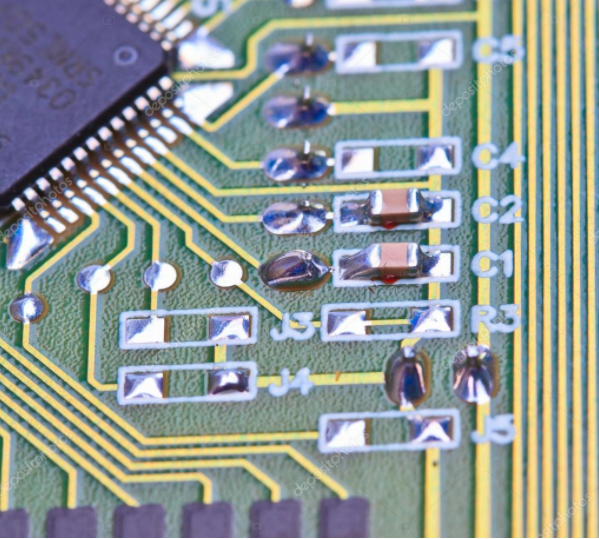
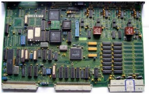
The function of the control unit designed in this article in the entire system is to transmit the coded signal received by the ground receiving device back to the main station data processing center. The specific working process is to first store the host computer data, and then through the bit error rate test and calculation, select a path with the lowest bit error rate as the data transmission path, and finally transmit the stored host computer data to the main station data processing center through this path To process. After comprehensive consideration, Altera's Cyclone II-2C8 was selected as the core chip, as well as externally expanded SDRAM, Flash, various input/output circuits and MAX232 interface chips, etc., and combined with Nios II soft-core processor development kit to achieve. The structure of the control unit is shown in Figure 1.

The clock frequency of CycloneII-2C8 is up to 150 MHz or more. Because the data storage area inside FPGA is relatively small, SDRAM is used to expand the external data storage space. SDRAM adopts Hy-nix Company's HY57V651610/SO, the clock frequency reaches above 75 MHz. Therefore, it is necessary to consider the signal integrity problems caused by the excessively high signal frequency. I chose the powerful Cad-ence design software, which integrates schematic design, PCB Layout, and high-speed simulation analysis. It can solve the problems related to electrical performance in all aspects of the design and greatly improve the design. Success rate.
2 Key signal topology and simulation
The higher frequency parts in this system are FPGA and SDRAM. The clock frequency of FPGA can reach more than 150 MHz, and the clock frequency of SDRAM can reach more than 75 MHz. Because the internal high frequency of FPGA has no effect on other devices, and the connection between FPGA and SDRAM is seamless, the signal integrity directly affects whether FPGA can read and write SDRAM correctly. In PCB design, the high-speed simulation tool SPECCTRAQuest of Cadence software is used, and the IBIS model of the device is used to analyze the signal integrity, and the impedance matching and topology structure are optimized to ensure the normal operation of the system. This article only gives a detailed explanation of signal reflection and crosstalk, and other simulations are similar.
2.1 Reflection
The transmitting end is 44 pins of HY57V561620, the receiving end is 60 pins of Cyclone II, and the excitation is a 66 MHz square wave. Figure 2 shows the topological structure, and Figure 3 shows the simulated waveform.

It can be seen from the simulation waveform that the waveform distortion is caused by the signal reflection, and the obvious ringing phenomenon is produced. The existence of the ringing phenomenon causes the signal to cross the level logic threshold many times, which leads to the disorder of the logic function. An effective way to reduce the ringing noise is to connect a small resistor in series with the circuit, which provides damping for the circuit, can significantly reduce the ringing amplitude and shorten the ringing oscillation time, while hardly affecting the circuit speed. In engineering use, the resistance is usually 33 Ω. Figure 4 and Figure 5 show the topological structure and simulated waveforms after the series resistance.

The ringing phenomenon after series resistance has been well solved. In fact, this solution is called impedance matching. Impedance occupies an extremely important position in the signal integrity problem.
2.2 Crosstalk
Extract SD_DQlO (connect 59 pins of Cyclone II and 45 pins of HY57V561620), SD_DQll (connect 58 pins of Cyclone II and 47 pins of HY57V561620), SD_DQ-l2 (connect 57 pins of Cyclone II and 48 pins of HY57V561620) Foot) these three networks to do crosstalk simulation between them. Among them, SD_DQll as the attacked network, SD_DQlO and SD_D-Ql2 as the attacking network. Their topology and simulation waveforms are shown in Figure 6 and Figure 7 (the parallel coupling length of the transmission line is L=1000 mil, and the pitch P=5 mil).

The simulation waveform is shown in Figure 8. It can be seen from Figure 7 that crosstalk has a great impact on the attacked network. The crosstalk value Crosstalk=657.95 mV is related to the parallel coupling length L and spacing P of the transmission line. The shorter the coupling length, the larger the spacing. The smaller the crosstalk. The simulation results are listed in Table 1.

Therefore, when making the PCB, the parallel length between the signal lines of different properties should be reduced as much as possible when allowed, the spacing between them should be widened, and the line width and height of some lines should be changed. Of course, there are many factors that affect crosstalk, such as current flow direction and frequency rise time of the interference source signal, which should be considered comprehensively.
Concluding remarks
In this high-speed PCB design of the control unit, the powerful Cadence software was used to achieve good results from the production of schematic diagrams, PCB layout to high-speed simulation analysis. According to the reasonable topology and layout obtained by SPEECTRAQuest simulation analysis, the circuit board can work normally. This design method greatly shortens the hardware debugging time, improves work efficiency, and saves design costs.