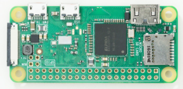
In this article, it mainly introduces the definition of the twelve levels of PCB board and describes their meaning
1. TOP LAYER (top wiring layer):
Designed as the top copper foil trace. If it is a single panel, there is no such layer.
2. BOMTTOM LAYER (bottom wiring layer):
Designed as bottom copper foil trace.
3. TOP/BOTTOM SOLDER (top/bottom solder mask green oil layer):
Apply solder mask green oil on the top/bottom layer to avoid tin on the copper foil and ensure insulation. Open the window with solder mask at the pads, vias and non-electrical traces on this layer.
In the design, the pad will be opened by default (OVERRIDE: 0.1016mm), that is, the pad exposes the copper foil and expands by 0.1016mm, and it will be tinned during wave soldering. It is recommended not to make design changes to ensure solderability;

The via hole will be opened by default in the design (OVERRIDE: 0.1016mm), that is, the via hole exposes the copper foil, expands by 0.1016mm, and will be tinned during wave soldering. If the design is to avoid tin on the vias and not expose the copper, you must check the PENTING option in the additional properties of the vias SOLDER MASK (solder mask opening), then close the via opening.
In addition, this layer can also independently carry out non-electrical wiring, and the solder mask green oil will open the window accordingly. If it is on a copper foil trace, it is used to enhance the overcurrent capability of the trace, and tin is added during welding; if it is on a non-copper foil trace, it is generally designed for logo identification and special character silk screen printing, which can be omitted Make the character silk screen layer.
4. TOP/BOTTOM PASTE (top/bottom solder paste layer):
This layer is generally used to apply solder paste during the SMT reflow process of SMT components, and it has nothing to do with the printed board manufacturer's board. It can be deleted when exporting GERBER, and the PCB design can ensure the default.
5. TOP/BOTTOM OVERLAY (top/bottom screen printing layer):
Designed as a variety of silk-screened logos, such as component number, characters, trademarks, etc.
6. MECHANICAL LAYERS (mechanical layer):
Designed as a PCB mechanical shape, the default LAYER1 is the shape layer. Other LAYER2/3/4, etc. can be used for mechanical size marking or special purposes. For example, when some boards need to be made of conductive carbon oil, LAYER2/3/4, etc. can be used, but the purpose of the layer must be clearly marked on the same layer.
7. KEEPOUT LAYER (prohibited wiring layer):
The design is to prohibit the wiring layer, and many designers also choose to make the mechanical shape of the PCB circuit board. If there are KEEPOUT and MECHANICAL LAYER1 on the PCB circuit board at the same time, it mainly depends on the completeness of the appearance of the two layers, usually based on the MECHANICAL LAYER1. It is recommended to choose MECHANICAL LAYER1 as the shape layer when designing. If you choose KEEPOUT LAYER as the shape, do not choose MECHANICAL LAYER1.
8. MIDLAYERS (middle signal layer):
It is mostly suitable for multi-layer boards, and can also be used as a special layer, but you must understand the role of the layer on the same layer.
9. INTERNAL PLANES (internal electrical layer):
Suitable for multi-layer boards.
10. MULTI LAYER (through hole layer):
Via pad layer.
11. DRILL GUIDE (drilling positioning layer):
The coordinate layer is positioned at the center of the hole of the pad and the via hole.
12. DRILL DRAWING (drilling description layer):
The description layer of the hole diameter of PCB pads and vias.